A safe distance warning device for automobiles in motion
A technology for automobile safety and warning devices, applied in signal devices, vehicle parts, transportation and packaging, etc., can solve the problems of speed sensors and ultrasonic sensors susceptible to clutter interference, anti-interference ability, low data accuracy, etc., and achieve anti-interference ability. Strong, high data accuracy, accurate data effect
- Summary
- Abstract
- Description
- Claims
- Application Information
AI Technical Summary
Problems solved by technology
Method used
Image
Examples
Embodiment 1
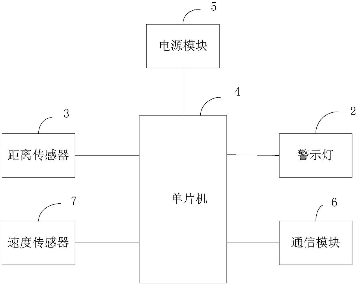
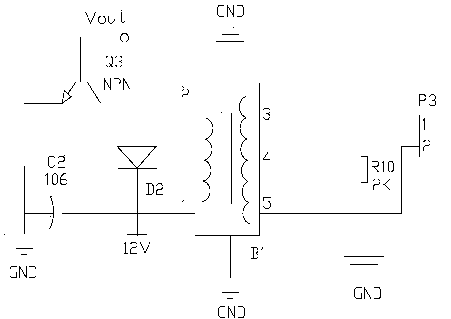
[0021] Such as Figure 1 to Figure 5 Shown, a kind of vehicle safety distance warning device in driving comprises single-chip microcomputer 4, power supply module 5, ultrasonic sensor 3, speed sensor 7, warning light 2, communication module 6; The level input end is connected, the distance signal receiving end of the single-chip microcomputer 4 is connected with the signal output end of the ultrasonic sensor 3, the speed signal receiving end of the single-chip microcomputer 4 is connected with the signal output end of the speed sensor 7, and the communication end of the single-chip microcomputer 4 is connected with the communication module 6. The control receiving end is connected, the light control end of the single-chip microcomputer 4 is connected with the control receiving end of the warning light 2, the ultrasonic sensor 3 is located at the rear side middle position of the automobile 1, and the described warning light 2 is located at both sides of the automobile 1 rear sid...
Embodiment 2
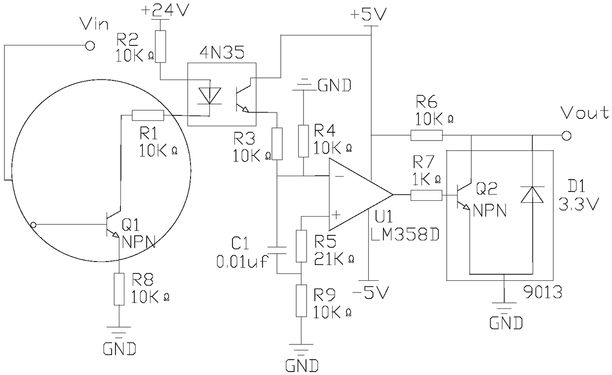
[0024] Such as Figure 1 to Figure 5 As shown, the difference between this embodiment and Embodiment 1 is that in the speed sensor 7, the voltage of +24V is grounded through the optocoupler 4N35, resistor R1, NPN transistor Q1, and resistor R8 in sequence, and the +5V voltage is grounded through the optocoupler 4N35 and the resistor R8. The first terminal of the resistor R3 is connected, the second terminal of the resistor R3 is connected to the negative input terminal of the integrated operational amplifier U1, and grounded after passing through the capacitor C1 and the resistor R9, and the positive input terminal of the integrated operational amplifier U1 is grounded after passing through the resistor R5 and the resistor R9 , the first terminal of the resistor R4 is connected to the negative input terminal of the integrated operational amplifier U1, the second terminal of the resistor R4 is grounded, the output terminal of the integrated operational amplifier U1 is connected ...
Embodiment 3
[0027] Such as Figure 1 to Figure 5 As shown, the difference between this embodiment and Embodiment 1 to Embodiment 2 is that the integrated operational amplifier U1 is an LM358D chip, and the resistance values of the resistors R1, R2, R3, R4, R6, R8, and R9 are equal. The resistance value of the resistor R5 is 10KΩ, the resistance value of the resistor R5 is 21KΩ, the resistance value of the resistor R7 is 1KΩ, and the capacitance C1 is 0.01uf.
PUM
 Abstract
Description
Claims
Application Information
 - R&D
- Intellectual Property
- Life Sciences
- Materials
- Tech Scout
- Unparalleled Data Quality
- Higher Quality Content
- 60% Fewer Hallucinations
Browse by: Latest US Patents, China's latest patents, Technical Efficacy Thesaurus, Application Domain, Technology Topic, Popular Technical Reports.
© 2025 PatSnap. All rights reserved.Legal|Privacy policy|Modern Slavery Act Transparency Statement|Sitemap|About US| Contact US: help@patsnap.com


