Dynamic high-flux measurement device for measuring bending and compression performances of microstructure of material
A material microscopic and measuring device technology, used in measuring devices, analyzing materials, and material analysis by optical means, etc., can solve the problems of unobservable microstructure changes, low accuracy, and meshing accuracy affecting simulation results.
- Summary
- Abstract
- Description
- Claims
- Application Information
AI Technical Summary
Problems solved by technology
Method used
Image

Examples
Embodiment 1
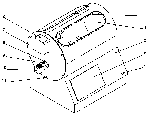
[0056]A dynamic high-throughput measurement device for bending and compressing properties of material microstructures, including a power switch 1, a touch control panel 2, a housing 3, a front observation window 4, a rear observation window 5, a front cover 7, a color filter 8, and an aperture diaphragm 9. Microscope light source 10, camera interface 12, rear guide rail 13, front guide rail 14, computer data interface 16, atmosphere input terminal 17, atmosphere output terminal 18, servo motor 26, reducer 27, left bracket 28, front slide bar 29, Slider 30, slider front sliding bearing 31, pressure head 32, pressure head front sliding bearing 33, displacement sensor 34, screw rod 36, slider rear sliding bearing 37, nut 38, support rod 39, rear sliding rod 40, pressure sensor Left support frame 41, pressure sensor 42, pressure sensor right support frame 43, rear sliding bearing 45 of pressure head, rear support seat 46, rear insulating sheet 47, front supporting seat 50, front in...
Embodiment 2
[0064] The structure of this embodiment is the same as that of Embodiment 1, except that the compression head 54 is replaced by a front curved support roller 62 and a rear curved support roller 58, the compression support platform 56 is replaced by a curved support platform 59, and the front curved support roller 62 is fixed on On the front insulating sheet 51, the rear bending support roller 58 is fixed on the rear insulating sheet 47, the left end of the bending support platform 59 is an arc-shaped structure, and the bending support platform 59 is fixed on the right bracket 52 through the dovetail groove; the three-point bending sample 63 Installed between the front bending support roller 62, the rear bending support roller 58 and the bending support table 59, the three-point bending sample metallographic observation area 60 is prepared on the upper end surface of the three-point bending sample 63, the objective lens 25 is focused on the metallographic observation, and the tem...
Embodiment 3
[0067] The structure of this embodiment is the same as that of Embodiment 1, the difference is that the compression indenter 54 is replaced by a V-shaped bending indenter 64, the compression support platform 56 is replaced by a V-shaped bending support platform 67, and the left end of the V-shaped bending support platform 67 is V V-shaped bending indenter 64 is fixed on the front insulating sheet 51 and rear insulating sheet 47, the V-shaped bending support table 67 is fixed on the right bracket 52 through the dovetail groove, and the V-shaped bending sample 65 is installed on the V-shaped bending indenter Between 64 and the V-shaped bending support platform 67 , the V-shaped curved metallographic observation area 66 is prepared from the V-shaped curved sample 65 , and the objective lens 25 is focused on the V-shaped curved metallographic observation area 66 .
[0068] The experimental material is ZCuPb30, the sample length is 30mm, the width is 8mm, and the thickness is 3mm. T...
PUM
 Abstract
Description
Claims
Application Information
 - R&D
- Intellectual Property
- Life Sciences
- Materials
- Tech Scout
- Unparalleled Data Quality
- Higher Quality Content
- 60% Fewer Hallucinations
Browse by: Latest US Patents, China's latest patents, Technical Efficacy Thesaurus, Application Domain, Technology Topic, Popular Technical Reports.
© 2025 PatSnap. All rights reserved.Legal|Privacy policy|Modern Slavery Act Transparency Statement|Sitemap|About US| Contact US: help@patsnap.com