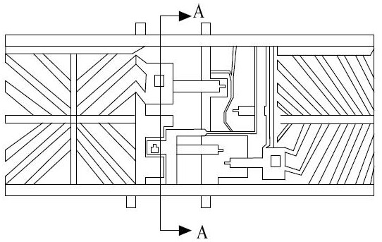
A kind of array substrate and display panel
An array substrate and thin-film transistor technology, applied in the field of display devices, can solve the problems of low aperture ratio and high risk of ITO climbing disconnection, and achieve the effect of increasing aperture ratio, reducing disconnection risk, and reducing design proportion
- Summary
- Abstract
- Description
- Claims
- Application Information
AI Technical Summary
Problems solved by technology
Method used
Image

Examples
Embodiment 1
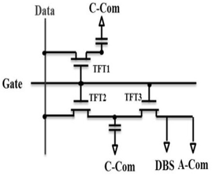
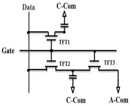
[0038] Based on Embodiment 1 of the present invention, Embodiment 2 of the present invention provides a display panel, which includes a color filter substrate, the aforementioned array substrate, and a liquid crystal display layer disposed between the array substrate and the color filter substrate.
[0039] The color filter substrate includes a glass substrate, and a common electrode layer C-com arranged on the glass substrate, and the common electrode layer C-com is made of indium tin oxide (ITO) on the entire surface.
[0040] Wherein, when the display panel is photo-matched, the common electrode layer C-com on the color filter substrate forms a first storage capacitor with the main pixel electrode, and forms a second storage capacitor with the slave pixel electrode. More specifically, the capacitance values of the first storage capacitor and the second storage capacitor are equal.
[0041] Specifically, when the liquid crystal panel is photo-matched, the voltage provided ...
PUM
 Abstract
Description
Claims
Application Information
 - R&D
- Intellectual Property
- Life Sciences
- Materials
- Tech Scout
- Unparalleled Data Quality
- Higher Quality Content
- 60% Fewer Hallucinations
Browse by: Latest US Patents, China's latest patents, Technical Efficacy Thesaurus, Application Domain, Technology Topic, Popular Technical Reports.
© 2025 PatSnap. All rights reserved.Legal|Privacy policy|Modern Slavery Act Transparency Statement|Sitemap|About US| Contact US: help@patsnap.com