Through silicon via stack-based three-stack memory structure and manufacturing method thereof

A through-silicon via and memory technology, which is applied in the field of memory, can solve the problems of large chip area, lower storage density, and smaller core area, and achieve the effects of saving area, reducing wiring density, and providing storage density

Pending Publication Date: 2019-02-01
YANGTZE MEMORY TECH CO LTD
View PDF12 Cites 15 Cited by
  • Summary
  • Abstract
  • Description
  • Claims
  • Application Information

AI Technical Summary

Problems solved by technology

In this three-dimensional memory structure, the through array contact (Through Array Contact) occupies a large chip area, which makes the area of ​​the core area smaller, thereby reducing the storage density; in addition, a large number of metal wirings are used to provide CMOS circuits and memory cell arrays. The increase in wiring density will affect the yield and reliability of the three-dimensional memory structure

Method used


Image

  • Through silicon via stack-based three-stack memory structure and manufacturing method thereof
  • Through silicon via stack-based three-stack memory structure and manufacturing method thereof
  • Through silicon via stack-based three-stack memory structure and manufacturing method thereof

Examples


Embodiment Construction

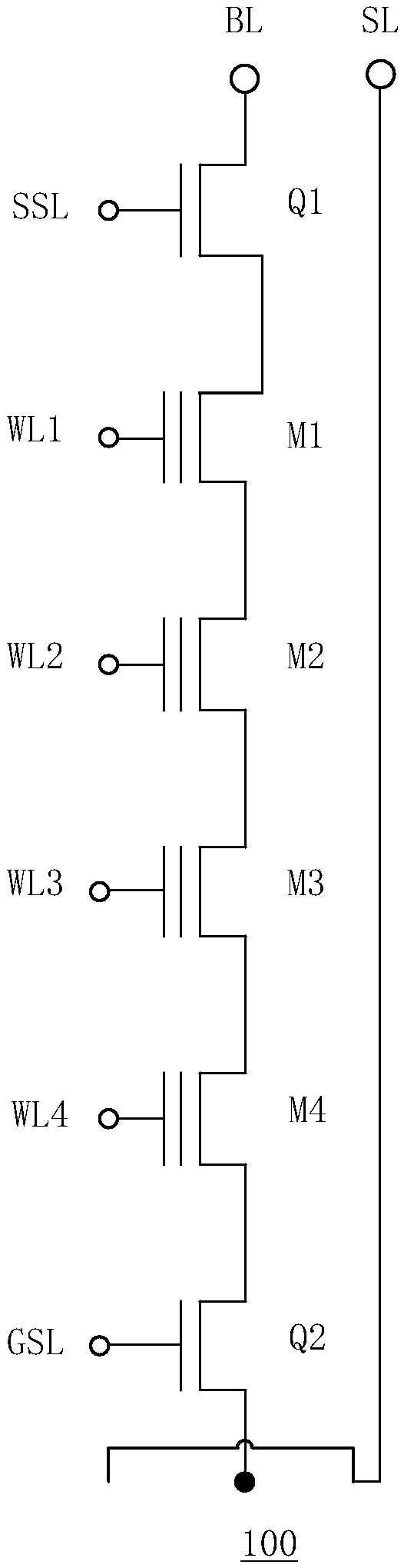
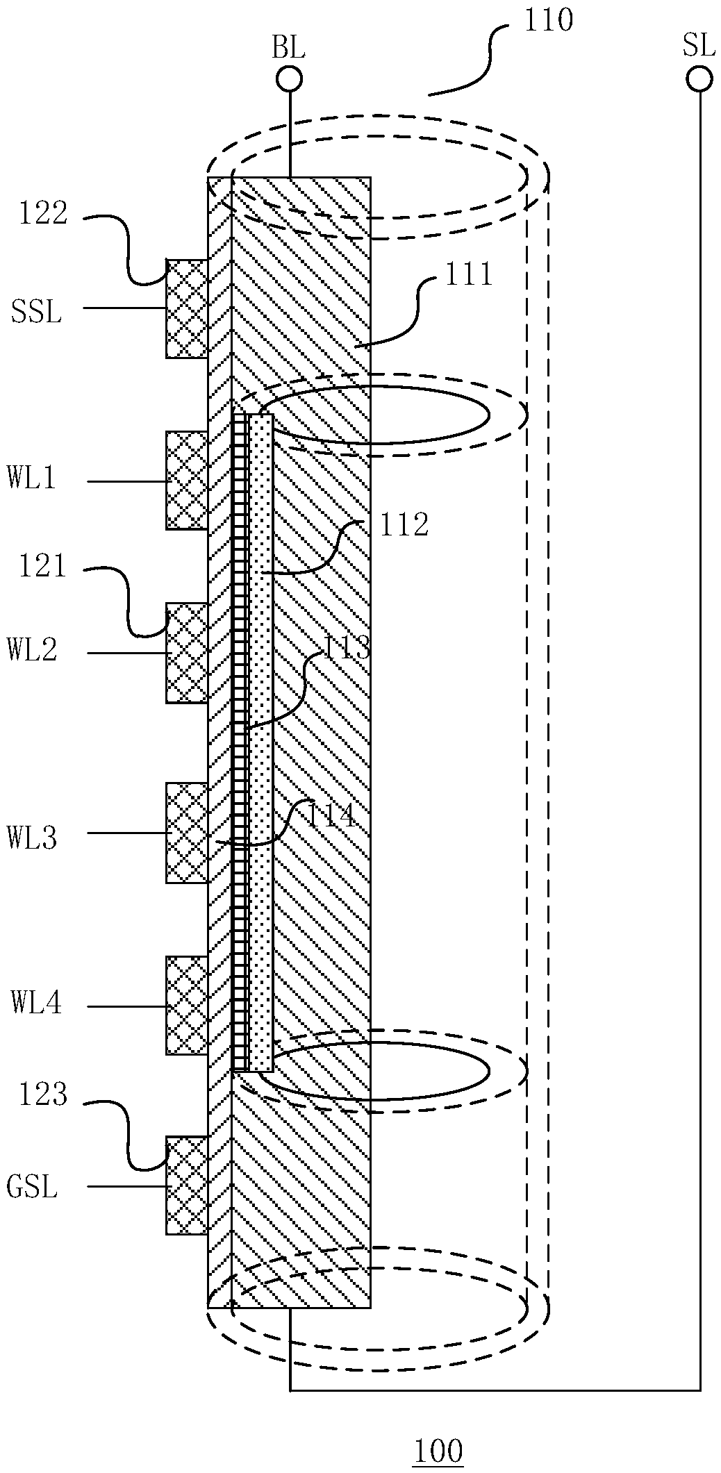
[0027] Hereinafter, various embodiments of the present invention will be described in more detail with reference to the accompanying drawings. In the various drawings, the same elements are represented by the same or similar reference numerals. For the sake of clarity, the various parts in the drawings are not drawn to scale.

[0028] The specific embodiments of the present invention will be described in further detail below in conjunction with the drawings and embodiments.

[0029] The "above" described in the present invention refers to being located above the plane of the substrate, which can refer to the direct contact between materials, or it can be arranged at intervals.

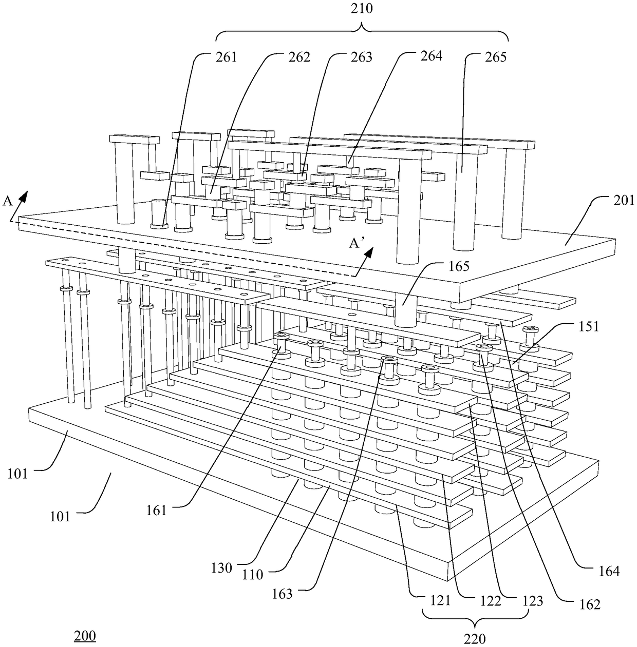
[0030] In the present application, the term "semiconductor structure" refers to a general term for the entire semiconductor structure formed in each step of manufacturing a memory device, including all layers or regions that have been formed. In the following, many specific details of the present invention ...


PUM


Abstract

The invention relates to a through silicon via stack-based three-stack memory structure. According to the through silicon via stack-based three-stack memory structure, a CMOS circuit comprises a firstsilicon substrate and a first insulating layer on the first silicon substrate, a plurality of first external pads being arranged in the first insulating layer; a memory cell array includes a second silicon substrate and a second insulating layer on the second silicon substrate, a plurality of second external pads being arranged in the second insulating layer; the CMOS circuit further comprises through silicon vias which pass through the first insulating layer and the first silicon substrate and are electrically connected with the first external pads; and the first silicon substrate and the second insulating layer contact with each other, the through silicon vias are bonded to the second external pads, and therefore, electrical connection between the CMOS circuit and the memory cell arraycan be realized. According to the through silicon via stack-based three-stack memory structure provided by the embodiments of the invention, the through silicon vias are formed on the CMOS circuit; the first ends of the through silicon vias are connected with the first external pads on the CMOS circuit, and the second ends of the through silicon vias are bonded to the second external pads of the memory cell array, so that the electrical connection between the CMOS circuit and the memory cell array is realized, and therefore, storage density can be improved, and wiring density can be decreased.

Description

Technical field [0001] The present invention relates to the field of memory technology, in particular to a three-stack memory structure based on TSV stacking and a manufacturing method. Background technique [0002] The improvement of the storage density of the storage device is closely related to the progress of the semiconductor manufacturing process. As the aperture of the semiconductor manufacturing process becomes smaller and smaller, the storage density of the memory device becomes higher and higher. In order to further increase the storage density, a storage device with a three-dimensional structure (ie, a three-dimensional memory structure) has been developed. The three-dimensional memory structure includes a plurality of memory cells stacked in a vertical direction, and the integration degree can be doubled on a unit area of ​​a wafer, and the cost can be reduced. [0003] In the three-dimensional memory structure of the NAND structure, one is to form a CMOS circuit firs...

Claims


Application Information

Patent Timeline
Patent Type & Authority Applications(China)
IPC IPC(8): H01L27/1157H01L27/11578
CPCH10B43/35H10B43/20
Inventor 胡斌肖莉红
Owner YANGTZE MEMORY TECH CO LTD
Why Eureka
Try Eureka