AlN film growing method

A thin film growth and thin film technology, which is applied in the direction of ion implantation plating, coating, electrical components, etc., can solve the problems of low production process output efficiency and insufficient process stability, so as to increase stability, prolong service life, improve The effect of productivity

Inactive Publication Date: 2019-02-12
LATTICE POWER (JIANGXI) CORP
View PDF3 Cites 2 Cited by
  • Summary
  • Abstract
  • Description
  • Claims
  • Application Information

AI Technical Summary

Problems solved by technology

[0004] In order to overcome the above deficiencies, the present invention provides an AlN thin film growth method, which effecti

Method used


Image

  • AlN film growing method

Examples


Embodiment 1

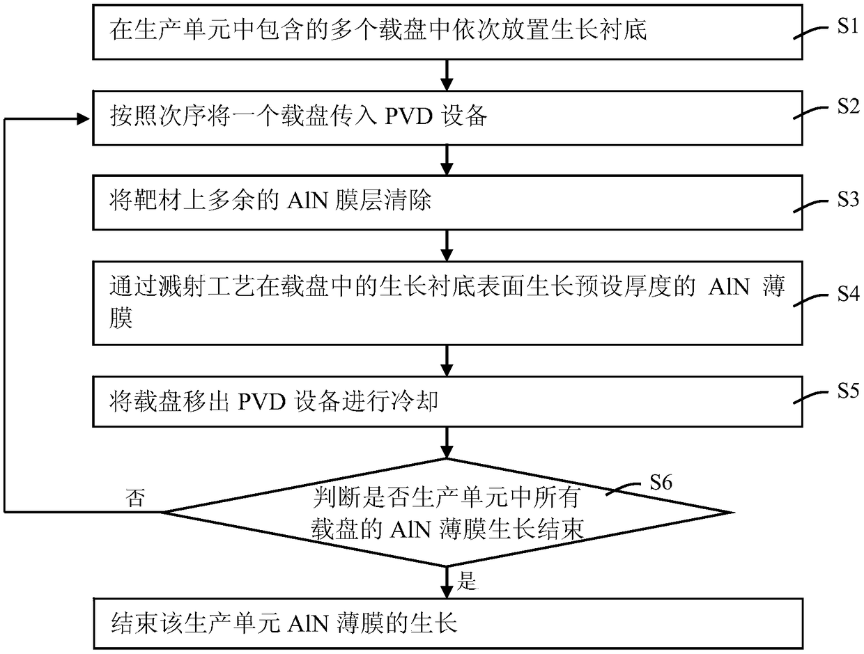
[0022] Adjust the voltage of magnetron sputtering produced by AlN in PVD equipment to 250-260V (volts), fill 7 SIC carriers with 5 pieces of 4-inch PSS substrates respectively, and place them in the same plug as a production unit ;Place the plug in the loading chamber and vacuumize it, use the mechanical arm to transfer the first carrier plate to the reaction chamber, when the vacuum degree in the reaction chamber reaches 10E-7torr, and the temperature is heated to 650°C to stabilize, the A baffle is introduced from above, 200sccm of Ar gas is introduced, and the sputtering DC power is 3000W for 15s to remove the AlN film on the target. After that, pass 35sccm of Ar gas, 175sccm of N 2 , 2sccm O 2 , the sputtering power is 3400W, the magnetron sputtering voltage is controlled between 250-260V, the baffle is removed, and a 30nm (nanometer) thick AlN film is plated on the PSS substrate. After the growth is over, transfer the carrier plate to the cooling chamber to cool down, t...

Embodiment 2

[0024] Adjust the magnetron sputtering voltage produced by AlN in the PVD equipment to 250-260V, fill the seven SIC carriers with five 4-inch PSS substrates respectively, and place them in the same card as a production unit. The plug is placed in the loading chamber and vacuumed, and the first disk is transferred to the reaction chamber by a robot arm. When the vacuum degree in the reaction chamber reaches 10E-7torr and the temperature is heated to 650°C and stabilizes, a disk is introduced above the reaction disk. The baffle is fed with 200 sccm of Ar gas, and the sputtering DC power is 2400W for 12s to remove a layer of AlN film on the target. After that, pass 35sccm of Ar gas, 175sccm of N 2 , 2sccm O 2 , The sputtering power is 3400W, the magnetron sputtering voltage is controlled between 250-260V, the baffle is removed, and a 15nm thick AlN film is plated on the PSS substrate. After the growth is over, transfer the carrier plate to the cooling chamber to cool down, then...


PUM


Abstract

The invention provides an AlN film growing method. The AlN film growing method comprises the following steps: S1, successively placing growing substrates in a plurality of carrying plates in a production unit; S2, transferring a carrying plate to PVD equipment in sequence; S3, removing a redundant AlN film layer on a target material; S4, growing an AlN film with a preset thickness on the surface of the growing substrate in the carrying plates through a sputtering process; S5, moving the carrying plates out of the PVD equipment and cooling the carrying plates; and S6, judging whether growing ofAlN films of all the carrying plates in the production unit is finished or not, if growing of the AlN films of all the carrying plates in the production unit is finished, finishing growth of the AlNfilm of the production unit, and if growing of the AlN films of all the carrying plates in the production unit is not finished, skipping to step S2. The circumstance that the follow-up sputtering process is affected due to the over-thick AlN layer on the target material is avoided effectively, continuous production can be carried out, the circumstance that the process of AlN removing and pre-settling at regular intervals is not required, the yield efficiency is greatly improved, and the stability of the process is improved.

Description

technical field [0001] The invention relates to the technical field of semiconductors, in particular to an AlN film growth method. Background technique [0002] When LED sapphire epitaxial wafers are grown in MOCVD (metal organic compound chemical vapor deposition), the process used is to deposit GaN / InGaN epitaxial layers on PSS (Patterned Sapphire Substrate, patterned sapphire substrate); due to the sapphire substrate and GaN film layer There is a problem of large lattice mismatch between them, and a GaN buffer layer is usually formed on a sapphire substrate first. However, the buffer layer is not beneficial to the LED device itself, but will absorb light during the working process of the LED device and reduce its brightness, and waste the machine time of MOCVD at the same time. In order to improve the efficiency of epitaxial growth, AlN (aluminum nitride) film layers were deposited on the PSS substrate instead of the GaN buffer layer to reduce the time for growing the bu...

Claims


Application Information

Patent Timeline
IPC IPC(8): H01L21/02H01L21/67C23C14/06C23C14/35
CPCC23C14/0617C23C14/35H01L21/0242H01L21/0243H01L21/0254H01L21/02631H01L21/02661H01L21/67253
Inventor 练发东涂逵
Owner LATTICE POWER (JIANGXI) CORP
Why Eureka
Try Eureka