Bimetal-layer annular-interdigital-electrode flip-chip LED chip and manufacturing method thereof

A technology of LED chips and interdigitated electrodes, which is applied in the direction of circuits, electrical components, semiconductor devices, etc., can solve the problems of uneven distribution of chip current, current aggregation, etc., and achieve the effects of free configuration, improved yield rate, and high production efficiency

Active Publication Date: 2019-02-12
JIUJIANG VOCATIONAL & TECHN COLLEGE
View PDF4 Cites 5 Cited by
  • Summary
  • Abstract
  • Description
  • Claims
  • Application Information

AI Technical Summary

Problems solved by technology

[0003] However, since the p and n electrodes of the flip-chip LED are on the same side of the chip, the current needs to be transmitted laterally, and the internal current of the chip is not evenly distributed, but there is an obvious current aggregation phenomenon around the p and n electrodes.

Method used


Image

  • Bimetal-layer annular-interdigital-electrode flip-chip LED chip and manufacturing method thereof
  • Bimetal-layer annular-interdigital-electrode flip-chip LED chip and manufacturing method thereof
  • Bimetal-layer annular-interdigital-electrode flip-chip LED chip and manufacturing method thereof

Examples


Embodiment Construction

[0035] The present invention will be further described below in conjunction with the drawings.

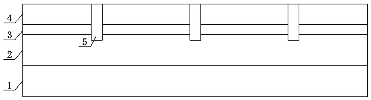
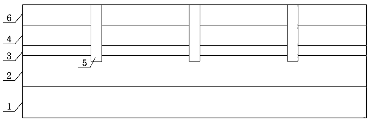
[0036] Such as Figure 5 to Figure 8 As shown, a double-metal layer ring-shaped interdigital electrode flip-chip LED chip includes a substrate 1, an n-type semiconductor layer 2, a light-emitting layer 3, and a p-type semiconductor layer 4 from bottom to top, on the p-type semiconductor layer 4 A current spreading layer 6 electrically connected to the p-type semiconductor layer 4 is provided, a first insulating isolation layer 7 insulated and connected to the current spreading layer 6 is provided on the current spreading layer 6, and the first insulating isolation layer 7 is divided into A plurality of n-pole annular belts distributed concentrically and equidistantly and a plurality of p-pole annular belts distributed concentrically and equidistantly, the n-pole annular belts and the p-pole annular belts are alternately arranged to form an annular interdigital structure;

[0037] A plu...


PUM


Abstract

The invention discloses a bimetal-layer annular-interdigital-electrode flip-chip LED chip and a manufacturing method thereof. The chip comprises a substrate, an n-type semiconductor layer, a light-emitting layer and a p-type semiconductor layer sequentially from bottom to top. The p-type semiconductor layer is provided with a current expanding layer which is provided with a first insulating isolation layer, the first insulating isolation layer is partitioned into a plurality of n-pole annular strips in concentric distribution at equal intervals and a plurality of p-pole annular strips in concentric distribution at equal intervals, and the n-pole annular strips and the p-pole annular strips are alternately arranged to form an annular interdigital structure. Different structural arrangementof the upper half portion and the lower half portion of each electrode is realized, electrode hindrance is sharply reduced, the problem of current gathering around the electrodes is solved, the current expanding performance of the flip-chip LED chip is improved, and accordingly light-emitting efficiency is improved. In addition, a large-area n electrode bonding pad and a p electrode bonding pad onthe upper half portion are realized, and accordingly free configuration is realized to a great extent, smooth implementation of subsequent packaging is facilitated, and the finished product rate is increased.

Description

Technical field [0001] The invention belongs to the technical field of semiconductor light-emitting devices, and particularly relates to a double-metal layer ring-shaped interdigitated electrode flip-chip LED chip and a manufacturing method thereof. Background technique [0002] Light emitting diodes (LEDs) are semiconductor light emitting devices made based on the principle of electroluminescence. Semiconductor lighting based on high-power LEDs is recognized as the third revolution in lighting history after incandescent lamps and fluorescent lamps. It has now been widely used in general lighting, entertainment lighting, agricultural lighting, sports lighting, commercial lighting, medical lighting, etc. In the field, the flip-chip structure LED is equivalent to inverting the horizontal structure LED, the chip connects the electrode with the heat dissipation substrate through the die bonding technology, and the photons are emitted into the air from the sapphire substrate side. Si...

Claims


Application Information

Patent Timeline
Patent Type & Authority Applications(China)
IPC IPC(8): H01L33/00H01L33/38H01L33/48H01L33/62
CPCH01L33/005H01L33/38H01L33/48H01L33/62
Inventor 吕家将江铃吴毅蒋晓刚王文超
Owner JIUJIANG VOCATIONAL & TECHN COLLEGE
Why Eureka
Try Eureka