Display panel and display device

A display panel and substrate technology, applied in nonlinear optics, instruments, optics, etc., can solve the problems of lowering the reliability of panel manufacturers' product quality, large differences in birefringence of liquid crystal molecules, and reducing the viewing effect of large viewing angles, etc., to achieve Good display effect, high penetration rate, and the effect of improving consumer satisfaction

Inactive Publication Date: 2019-02-15
HUIZHOU CHINA STAR OPTOELECTRONICS TECHNOLOGY CO LTD
View PDF7 Cites 6 Cited by
  • Summary
  • Abstract
  • Description
  • Claims
  • Application Information

AI Technical Summary

Problems solved by technology

However, since the VA-type liquid crystal display panel uses vertically rotating liquid crystals, the difference in birefringence of liquid crystal molecules is relatively large, resulting in serious color shift problems at large viewing angles.
In other words, in the same sub-pixel of the LCD panel, the gap between the two glass substrates (cell gap) is the same, and the tilting state of the liquid crystal molecules after being subjected to voltage is also the same, so that the color difference seen from different angles of the VA-type LCD panel is different. Larger, resulting in picture distortion, thereby reducing the user's viewing effect for large viewing angles, and also reducing the reliability of the panel manufacturer's product quality
[0004] Therefore, it is necessary to provide a display panel and a display device to solve the problem of color shift under large viewing angles in the prior art

Method used


Image

  • Display panel and display device
  • Display panel and display device
  • Display panel and display device

Examples


Embodiment Construction

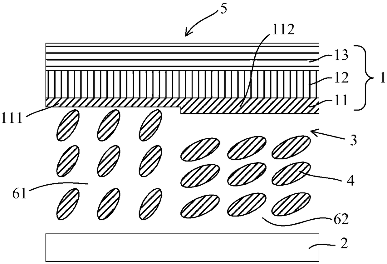
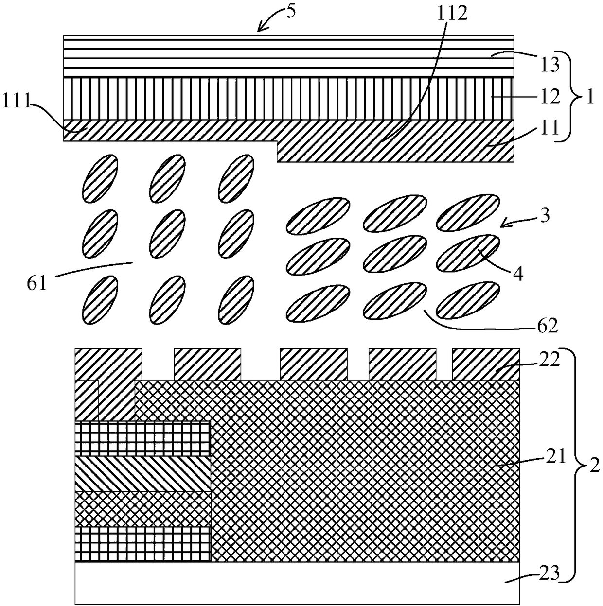
[0019] Reference in the detailed description to "an embodiment" means that a particular feature, structure, or characteristic described in connection with the embodiment can be included in at least one embodiment of the invention. The same terms appearing in different positions in the specification are not necessarily limited to the same implementation, but should be understood as independent or alternative implementations from other embodiments. Inspired by the technical solutions disclosed in the embodiments provided in the present invention, those skilled in the art should understand that the embodiments described in the present invention may have other combinations or changes of technical solutions consistent with the concept of the present invention.

[0020] The following descriptions of the various embodiments refer to the accompanying drawings to illustrate specific embodiments in which the present invention can be practiced. The directional terms mentioned in the pres...


PUM


Abstract

The invention discloses a display panel and a display device, wherein the display panel comprises a color film substrate and an array substrate arranged opposite to the color film substrate. A gap isformed between the color film substrate and the array substrate, the gap is filled with liquid crystal, the color film substrate defines a plurality of pixel areas, the color film substrate comprisesa transparent photoresist, the transparent photoresist is provided with a first photoresist layer and second photoresist layer corresponding to each pixel area, the first photoresist layer and the second photoresist layer divide the pixel areas into a first domain area and a second domain area, and the gap in the first domain area is larger than the gap in the second domain area. According to theinvention, liquid crystal gaps of different domain areas are formed in each pixel area through different photoresist layer thicknesses, so that the problem of large visual color cast is solved.

Description

technical field [0001] The invention relates to the field of display technology, in particular to a display panel and a display device. Background technique [0002] A liquid crystal display (Liquid Crystal Display, LCD) is usually composed of a color filter (Color Filter, CF) substrate, a thin film transistor (Thin Film Transistor, TFT) array substrate, and a liquid crystal layer (Liquid Crystal Layer, LC Layer) arranged between the two substrates. ) constitutes. The working principle of the liquid crystal display is to control the rotation of the liquid crystal molecules in the liquid crystal layer by applying a driving voltage on the two glass substrates, and refract the light from the backlight module to produce a picture. [0003] As far as LCDs currently on the market are concerned, they can be divided into three types, namely twisted nematic (Twisted Nematic, TN) or super twisted nematic (Super Twisted Nematic, STN) type, in-plane switching (In-Plane Switching, IPS ...

Claims


Application Information

Patent Timeline
Patent Type & Authority Applications(China)
IPC IPC(8): G02F1/1335
CPCG02F1/133514
Inventor 陈俊吉
Owner HUIZHOU CHINA STAR OPTOELECTRONICS TECHNOLOGY CO LTD
Why Eureka
Try Eureka