Eureka AIR delivers breakthrough ideas for toughest innovation challenges, trusted by R&D personnel around the world.

Low-temperature drift band gap reference voltage circuit and method, and chip of circuit

A technology of reference voltage and low temperature drift, which is applied in the direction of adjusting electrical variables, control/regulating systems, instruments, etc., and can solve the problems of inaccurate reference voltage, poor compensation accuracy, and poor high-order temperature compensation accuracy.

Active Publication Date: 2019-02-15
西安电子科技大学重庆集成电路创新研究院
View PDF4 Cites 14 Cited by
  • Summary
  • Abstract
  • Description
  • Claims
  • Application Information

AI Technical Summary

Problems solved by technology

[0013] 1) As the temperature changes, the bias current provided to the bandgap voltage generating circuit usually changes, resulting in inaccurate final output reference voltage
[0014] 2) The circuit design itself will cause poor compensation accuracy due to mismatch;
[0015] 3) The actual bandgap reference high-order temperature compensation accuracy is poor due to too rough theoretical approximation results of some circuits

Method used


Image

  • Low-temperature drift band gap reference voltage circuit and method, and chip of circuit
  • Low-temperature drift band gap reference voltage circuit and method, and chip of circuit
  • Low-temperature drift band gap reference voltage circuit and method, and chip of circuit

Examples


Embodiment 1

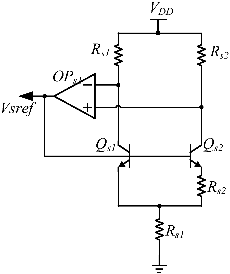
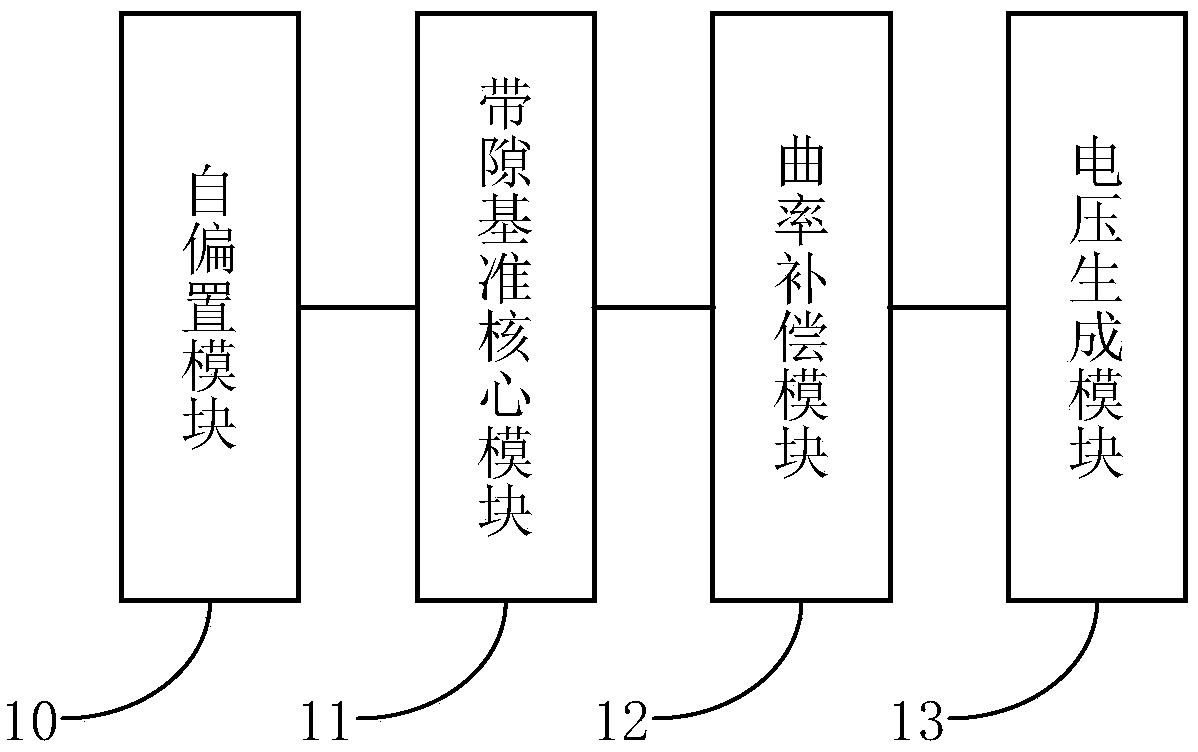
[0088] Such as Figure 4 As shown in Embodiment 1 of the low-temperature drift bandgap reference voltage circuit, the Figure 4 It can be known that Embodiment 1 includes a self-bias module 10 , a bandgap reference core module 11 and a voltage generation module 13 .

[0089] Self-bias module 10 includes field effect transistors (MOS transistors) M5 and M6; transistors Q3 and Q4, resistors R6 and R7; field effect transistors M5 and M6 are PMOS transistors; transistor Q3 is a PNP transistor, and transistor Q4 is an NPN transistor.

[0090] The sources of the field effect transistors M6 and M5 are connected to the power supply VDD, and the gate of the field effect transistor M5 is connected to the gate of the M6 ​​and the drain of the M5; the field effect transistors M6 and M5 form a current mirror; the drain of the field effect transistor M6 and One end of the resistor R7 is connected to point C and connected to the bandgap reference core module 11 as the first output of the se...

Embodiment 2

[0121] The preferred embodiment 2 of the present invention is an improvement based on the preferred embodiment 1. For parts not mentioned in this embodiment, reference may be made to the corresponding content in the first embodiment.

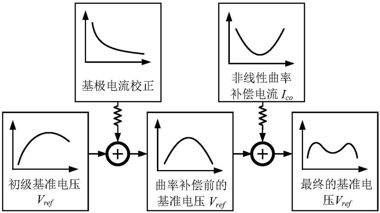
[0122] After the above-mentioned temperature compensation of the base current correction resistor, the output voltage Vref obtained has a parabolic linear variation trend with a downward curvature, and already has a lower temperature drift coefficient. In order to further improve the temperature drift tendency of the output voltage Vref under high temperature and low temperature conditions, it is considered to add a curvature compensation module in the circuit to compensate Vref. The proposed curvature compensation method adopts the idea of ​​dynamic adjustment, and continuously adjusts the magnitude of the compensation current Ico by monitoring the change of the positive temperature coefficient voltage VPTAT (proportional to absolute temperature...

Embodiment 3

[0146] Preferred Embodiment 3 of the present invention is an improvement based on Preferred Embodiment 1 and Preferred Embodiment 2. For parts not mentioned in this embodiment, reference may be made to the corresponding content in Preferred Embodiment 1 and Preferred Embodiment 2.

[0147] On the basis of the above preferred embodiment 1 and embodiment 2, in order to avoid performance degradation caused by process variation or mismatched circuit, a trimming circuit is added in the structure to correct the circuit after production.

[0148] Such as Figure 8 As shown in the third embodiment of the low-temperature drift bandgap reference voltage circuit of the present invention, the Figure 8 It can be seen that the trimming circuit for the temperature drift coefficient in the bandgap reference core module 11 includes two potentiometers Rt1 and Rt2, and their contact ports are respectively connected to the input terminals Vinp and Vinn of the amplifier OP1. What needs to be exp...


PUM


Abstract

The invention provides a low-temperature drift band gap reference voltage circuit and method, and a chip of the circuit. The circuit comprises a self-biasing module, a band gap reference core module and a voltage generation module. The method comprises the following steps of generating a primary reference voltage; generating a reference voltage before compensation through base current correction and the primary reference voltage; and generating a low-temperature drift band gap reference voltage. The low-temperature drift band gap reference voltage circuit and method is applied to a power management chip. The method has the advantages that the band gap reference voltage source circuit with ultrahigh precision and an ultralow-temperature drift coefficient is realized, and the high-stabilityreference voltage can be provided for circuit applications with relatively high reference voltage requirements.

Description

technical field [0001] The invention relates to the field of designing electronic circuits, and in particular relates to a low-temperature drift bandgap reference voltage circuit, a method and a chip thereof. Background technique [0002] At present, the reference voltage source has been used as an indispensable basic module in semiconductor integrated circuits, and it is widely used in amplifiers, analog-to-digital converters, digital-to-analog converters, radio frequency, sensors and power management chips. Traditional reference voltage sources include voltage references based on the reverse breakdown characteristics of zener diodes, voltage references based on PN junction forward conduction characteristics, and bandgap references. Among them, the bandgap reference has a simple structure and low voltage Stability and other advantages, therefore, have been widely used. [0003] With the development of semiconductor technology and portable electronic products, the demand fo...

Claims


Application Information

Patent Timeline
IPC IPC(8): G05F1/567
CPCG05F1/567
Inventor 朱光前张启东杨银堂
Owner 西安电子科技大学重庆集成电路创新研究院
Why Eureka
Eureka Blog
Learn More