Method for coupling silicon-based optoelectronic chip and single-mode optical fiber
An optoelectronic chip and single-mode fiber technology, which is applied to the coupling of optical waveguides, light guides, optics, etc., can solve the problems of low coupling efficiency between single-mode fiber and silicon waveguide, and achieve the effect of improving coupling tolerance and improving coupling efficiency.
- Summary
- Abstract
- Description
- Claims
- Application Information
AI Technical Summary
Problems solved by technology
Method used
Image

Examples
Embodiment 1
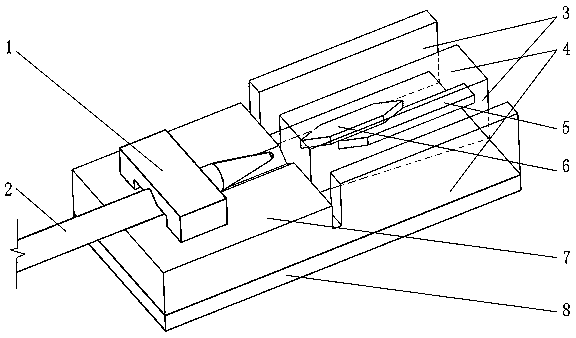
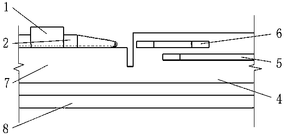
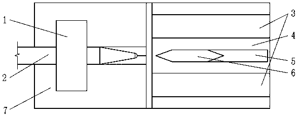
[0028] A coupling method between a silicon-based optoelectronic chip and a single-mode optical fiber 2, which is applied to the coupling between the single-mode optical fiber 2 and the silicon waveguide 5, such as figure 1 As shown, it is a schematic diagram of the coupling structure of Embodiment 1, such as figure 2 As shown, it is a schematic side sectional view of the coupling structure of Embodiment 1, such as image 3As shown, it is a top view of the coupling structure of Embodiment 1. In this embodiment, a silicon dioxide layer 4 is deposited and grown on a silicon substrate 8, a silicon waveguide 5 is disposed in the silicon dioxide layer 4, and the end face of the single-mode optical fiber 2 is processed into a convex curved surface. There is a gap between the single-mode optical fiber 2 and the silicon dioxide layer 4, and at least a section of low-refractive-index waveguide 6 is arranged between the single-mode optical fiber 2 and the silicon waveguide 5. is a shar...
Embodiment 2
[0031] A coupling method between a silicon-based optoelectronic chip and a single-mode optical fiber 2. In this embodiment, the installation process of the single-mode optical fiber 2 has been specifically improved, such as Figure 4 As shown, it is the structural diagram of the optical fiber installer in Embodiment 2, such as Figure 5 As shown, it is a schematic structural diagram of the execution part of the fiber mounter in Embodiment 2. The single-mode fiber 2 is installed to the coupling position through the fiber mounter. A slide bar 16, a slider 13, an optical fiber clamping seat 17 and an optical fiber clamping block 11, the optical fiber clamping seat 17 is fixedly connected with the slider 13, and the optical fiber clamping block 11 is closely attached to and fixedly connected with the optical fiber clamping seat 17 There are V-shaped grooves at the same position on the contact surface of the optical fiber clamping block 11 and the optical fiber clamping seat 17, th...
Embodiment 3
[0033] A coupling method between a silicon-based optoelectronic chip and a single-mode optical fiber 2. In this embodiment, the installation process of the single-mode optical fiber 2 has been specifically improved, such as Figure 6 As shown, it is a structural schematic diagram of the anti-collision device of the optical fiber mounter in Embodiment 3. The optical fiber mounter used when installing the single-mode optical fiber 2 to the coupling position in this embodiment also includes an anti-collision device, and the anti-collision device is at the output end of the single-mode optical fiber 2 Slider 13 is locked when moving to the coupled position. The refractive index difference between the silicon waveguide 5 and silicon dioxide is huge, so the silicon waveguide 5 used in conjunction with silicon dioxide has a strong binding effect on light, so the silicon waveguide 5 can have a smaller size, usually only a dozen The size is too small to tens of microns, and its ability...
PUM
 Abstract
Description
Claims
Application Information
 - Generate Ideas
- Intellectual Property
- Life Sciences
- Materials
- Tech Scout
- Unparalleled Data Quality
- Higher Quality Content
- 60% Fewer Hallucinations
Browse by: Latest US Patents, China's latest patents, Technical Efficacy Thesaurus, Application Domain, Technology Topic, Popular Technical Reports.
© 2025 PatSnap. All rights reserved.Legal|Privacy policy|Modern Slavery Act Transparency Statement|Sitemap|About US| Contact US: help@patsnap.com