2d TMDs-conducting polymer composites, their preparation methods and applications
A technology of conductive polymers and composite materials, applied in semiconductor/solid-state device manufacturing, circuits, electrical components, etc., can solve problems such as affecting hole injection ability, easy agglomeration, etc., to promote fast transport, prevent agglomeration, and excellent electrochemical performance. performance effect
- Summary
- Abstract
- Description
- Claims
- Application Information
AI Technical Summary
Problems solved by technology
Method used
Image

Examples
preparation example Construction
[0028] Correspondingly, an embodiment of the present invention provides a method for preparing a 2D TMDs-conductive polymer composite material, comprising the following steps:
[0029] S01. dispersing 2D TMDs and conductive polymers in an organic solvent to form a dispersion;
[0030] S02. ultrasonically treating the dispersion to prepare a 2D TMDs-conductive polymer composite.
[0031]The preparation method of the 2D TMDs-conductive polymer composite material provided by the embodiment of the present invention uses the ultrasonic exfoliation-intercalation method. The strong Π-Π stacking and electrostatic repulsion between the conductive polymer and the 2D TMDs basal surface can simultaneously realize the peeling and dispersion of 2D TMDs and the intercalation of conductive polymers between the 2D TMDs sheets. The 2D TMDs-conducting polymer composite prepared by ultrasonic exfoliation-intercalation method is conducive to better exerting the intrinsic properties of 2D TMDs and...
Embodiment 1
[0078] A kind of MoS 2 The preparation method of / SPAN nanocomposite material, comprises the following steps:
[0079] MoS 2 -Preparation of SPAN nanocomposites: 0.5mg MoS 2 and 0.5mg SPAN were dispersed in 100mL N,N-dimethylformamide (DMF), fully stirred, ultrasonically treated for 8h, and the upper layer suspension was centrifuged at 1500rpm for 20min to remove unstripped MoS 2 , the obtained homogeneous suspension is MoS 2 - SPAN nanocomposites.
Embodiment 2
[0081] A method for preparing a QLED device, comprising the following steps:
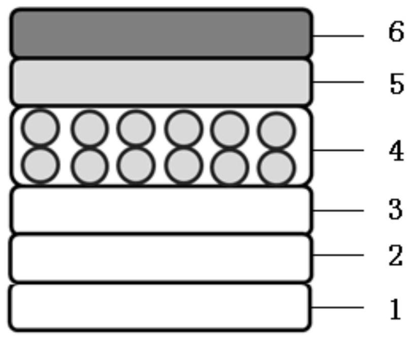
[0082] The patterned ITO substrate was sequentially placed in acetone, washing solution, deionized water and isopropanol for ultrasonic cleaning, each time for 15 minutes. After the ultrasound is completed, place the ITO in a clean oven to dry for later use. After the ITO substrate was dried, the ITO surface was treated with UV-ozone for 5 minutes.
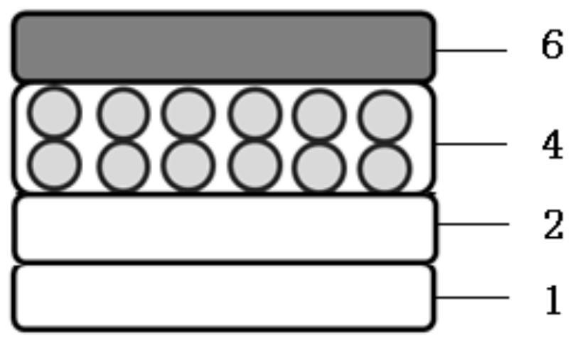
[0083] MoS at a concentration of 0.1 mg / ml 2 The / SPAN nanocomposite solution was deposited on the surface of the treated ITO substrate with a thickness of 30nm, and the substrate was placed on a heating stage at 150°C for 30 minutes to remove the solvent.
[0084] The substrate deposited with the hole injection layer was placed in a nitrogen atmosphere, a layer of TFB hole transport layer with a thickness of 30 nm was deposited, and the substrate was placed on a heating stage at 150° C. for 30 minutes to remove the solvent.
[0085] After the sheet ...
PUM
| Property | Measurement | Unit |
|---|---|---|
| concentration | aaaaa | aaaaa |
| thickness | aaaaa | aaaaa |
Abstract
Description
Claims
Application Information
 - R&D
- Intellectual Property
- Life Sciences
- Materials
- Tech Scout
- Unparalleled Data Quality
- Higher Quality Content
- 60% Fewer Hallucinations
Browse by: Latest US Patents, China's latest patents, Technical Efficacy Thesaurus, Application Domain, Technology Topic, Popular Technical Reports.
© 2025 PatSnap. All rights reserved.Legal|Privacy policy|Modern Slavery Act Transparency Statement|Sitemap|About US| Contact US: help@patsnap.com