
Substrate, preparation method thereof and display panel

A substrate and area technology, applied in semiconductor/solid-state device manufacturing, electrical components, electrical solid-state devices, etc., can solve problems such as large area and storage capacitor occupation

Active Publication Date: 2019-03-05
BOE TECH GRP CO LTD
View PDF5 Cites 5 Cited by
  • Summary
  • Abstract
  • Description
  • Claims
  • Application Information

AI Technical Summary

Problems solved by technology

However, in each sub-pixel, in addition to the TFT (Thin Film Transistor, thin film transistor), the storage capacitor (Cst) will also occupy a larger area

Method used


Image

  • Substrate, preparation method thereof and display panel
  • Substrate, preparation method thereof and display panel
  • Substrate, preparation method thereof and display panel

Examples


Embodiment Construction

[0046] The following will clearly and completely describe the technical solutions in the embodiments of the present invention with reference to the accompanying drawings in the embodiments of the present invention. Obviously, the described embodiments are only some, not all, embodiments of the present invention. Based on the embodiments of the present invention, all other embodiments obtained by persons of ordinary skill in the art without making creative efforts belong to the protection scope of the present invention.

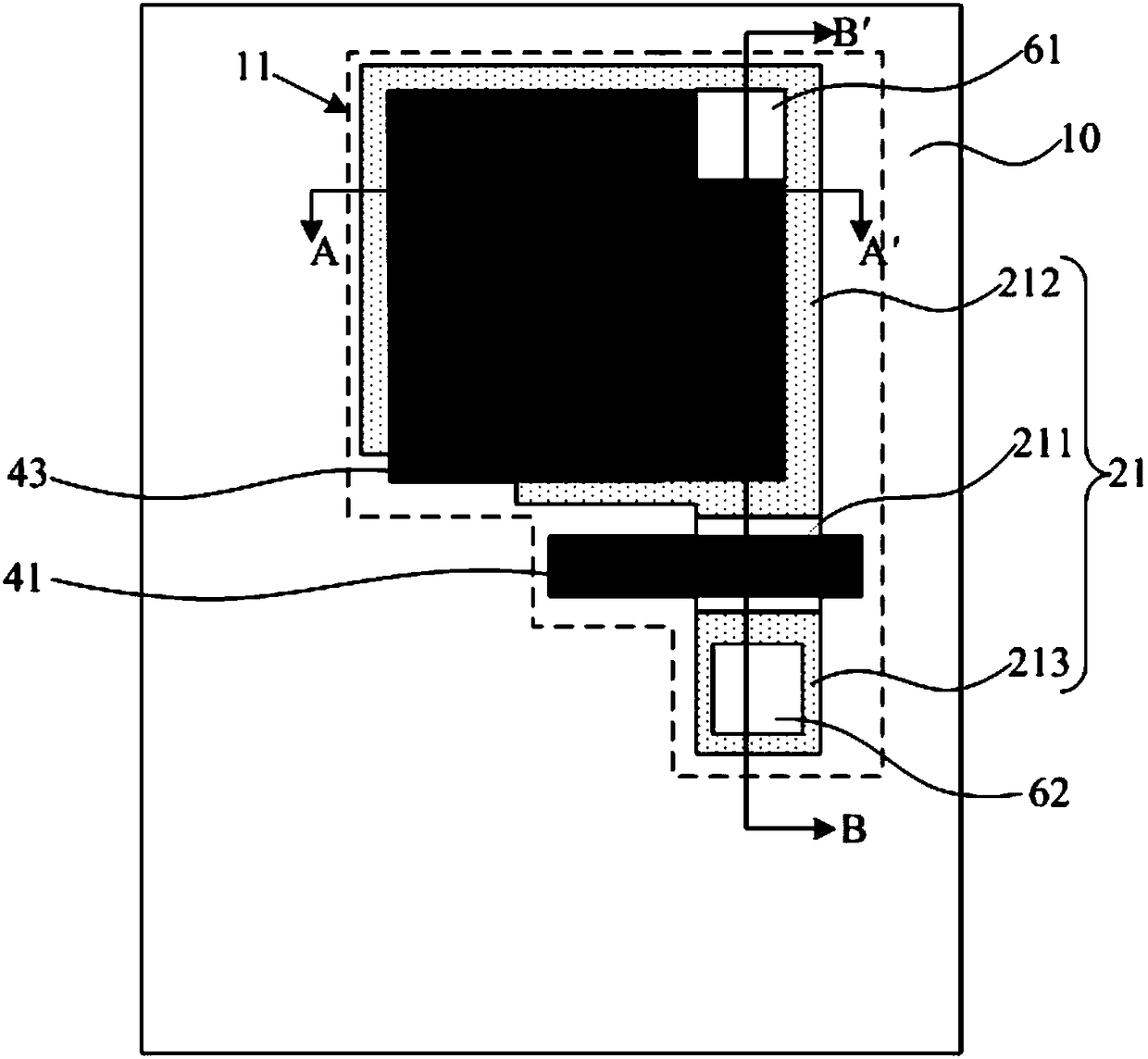
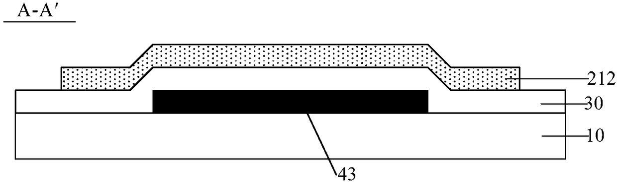
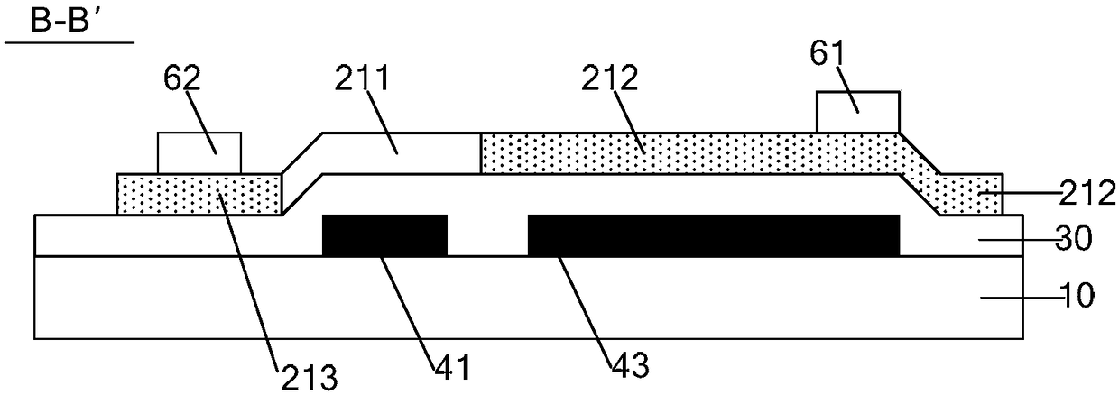
[0047] An embodiment of the present invention provides a substrate, such as Figure 1a-Figure 1c , Figure 2a-Figure 2c As shown, it includes a substrate 10 and a first TFT 11 disposed on each sub-pixel region on the substrate 10; the first TFT 11 includes a first active layer 21 and a first gate 41; the first active layer 21 includes a first active layer 21 The source region 211, the first conductorized region 212 and the second conductorized region 213 loca...


PUM


Abstract

The embodiment of the invention provides a substrate, a preparation method thereof and a display panel, relates to the technical field of display, and can reduce the area occupied by a storage capacitor, thereby improving the resolution. The substrate includes a base, and a first TFT disposed on each sub-pixel region of the base; the first TFT includes a first active layer and a first gate. The first active layer comprises a first active region, a first conductive region and a second conductive region located on both sides of the first active region, wherein the area of the first conductive region is larger than the area of the second conductive region; an orthographic projection of the first active region on the base at least partially overlaps with an orthographic projection of the firstgate on the base; the substrate further includes capacitive electrodes of which orthogonal projections on the base at least partially overlap with the orthogonal projections of the first conductive regions on the base; the capacitive electrodes are electrically connected to the first gate; and the capacitive electrodes and the first active layer are isolated by gate insulation layers.

Description

technical field [0001] The invention relates to the field of display technology, in particular to a substrate, a preparation method thereof, and a display panel. Background technique [0002] With the development of display technology, display devices are developing toward high resolution. However, in each sub-pixel, in addition to a TFT (Thin Film Transistor, thin film transistor), a storage capacitor (Cst) also occupies a larger area. Therefore, on the basis of meeting the capacitance value required by the display, how to reduce the area occupied by the storage capacitor and thereby improve the resolution has always been a difficult problem. Contents of the invention [0003] Embodiments of the present invention provide a substrate, a manufacturing method thereof, and a display panel, which can reduce the area occupied by storage capacitors, thereby improving resolution. [0004] In order to achieve the above object, embodiments of the present invention adopt the follo...

Claims


Application Information

Patent Timeline
IPC IPC(8): H01L27/12H01L21/84H01L27/32
CPCH01L27/124H01L27/1255H01L27/1259H10K59/1213H10K59/1216H01L29/78624H01L27/1225H01L27/1222H10K59/123H10K59/124
Inventor 宋振王国英
Owner BOE TECH GRP CO LTD
Learn More