Viewing angle switching architecture, method thereof and liquid crystal display device

A technology of viewing angle and display mode, which is applied in the field of liquid crystal display, can solve the problem of not supporting two sets of gamma voltage switching, and achieve the effect of improving image quality

Active Publication Date: 2019-03-08
KUSN INFOVISION OPTOELECTRONICS
9 Cites 1 Cited by

AI-Extracted Technical Summary

Problems solved by technology

[0005] In view of this, the purpose of the present invention is to provide a viewing angle switching architecture, which can solve the...

Method used

[0039] Finally, the source driver module 400 can drive and output corresponding pixel signals according to the second group of gamma voltage Gamma2 and the third group of gamma voltage Gamma3 alternately output by the second processing module 300, so as to meet the requirements of the second display mode. The image display requirements are met, thereby effectively improving the image quality of the display image of the liquid crystal display device.
[0055] The viewing angle switching method of the present embodiment can support three sets of gamma voltages, and supports switching between two sets of gamma voltages in a display mode, thereby effectively i...

Abstract

The invention provides a viewing angle switching architecture, a method thereof and a liquid crystal display device thereof. The view switching architecture includes a timing control module, a first processing module, a second processing module, and a source driving module. The timing control module outputs a voltage call command, a first polarity control signal, and a second polarity control signal according to a mode control signal, and the first processing module outputs a first voltage generation command and a reset signal. The second processing module executes the first voltage generationcommand to output a plurality of external supply voltages, and a second group of gamma voltages and a third group of gamma voltages are alternately output to the source driving module according to the second polarity control signal. The source driving module receives the voltage call command and uses the internal gamma correction circuit, a plurality of external supply voltages can be received toobtain a first group of gamma voltages. The view switching architecture can support three groups of gamma voltages and support the switching use of two groups of gamma voltages in one display mode, and effectively improves the image quality of a display screen of a liquid crystal display device.

Application Domain

Technology Topic

Image

  • Viewing angle switching architecture, method thereof and liquid crystal display device
  • Viewing angle switching architecture, method thereof and liquid crystal display device
  • Viewing angle switching architecture, method thereof and liquid crystal display device

Examples

  • Experimental program(4)

Example

[0025] First embodiment
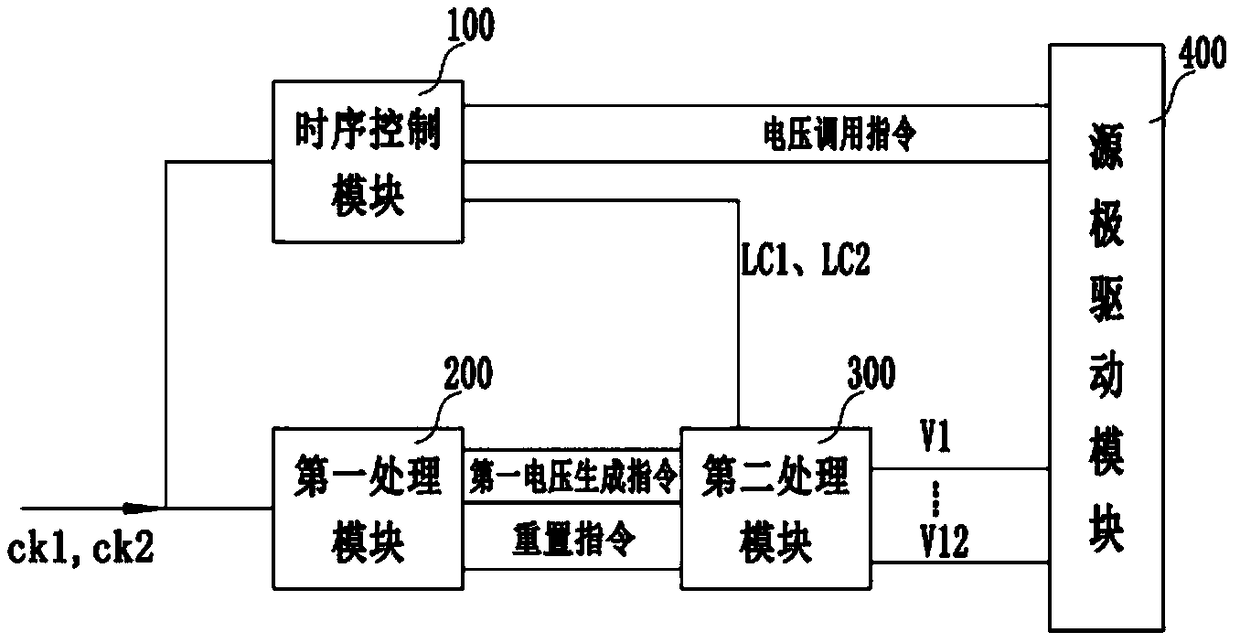
[0026] Please refer to figure 2 , figure 2 It is a schematic circuit diagram of the viewing angle switching architecture of the first embodiment. Such as figure 2 As shown, the perspective switching architecture of this embodiment includes a timing control module 100, a first processing module 200, a second processing module 300, and a source driving module 400. Wherein, the timing control module 100 outputs the voltage calling instruction and the first polarity control signal LC1 according to the first display mode control signal ck1, and outputs the second polarity control signal LC2 according to the second display mode control signal ck2. The first processing module 200 outputs a first voltage generation instruction according to the first display mode control signal ck1, and outputs a reset signal according to the second display mode control signal ck2. The second processing module 300 receives the first polarity control signal LC1 and the first voltage generation command, executes the first voltage generation command, outputs a plurality of externally supplied voltages, resets according to the reset signal, and according to the second polarity control signal LC2 The second group of gamma voltage Gamma2 and the third group of gamma voltage Gamma3 are alternately output to the source driving module 400 periodically. The source driving module 400 receives the voltage call instruction, and uses the gamma correction circuit inside the source driving module 400, and then receives a plurality of external supply voltages to obtain the first group of gamma voltage Gamma1; the source driving module 400 according to the first The group gamma voltage Gamma1, the second group gamma voltage Gamma2 or the third group gamma voltage Gamma3 drives the output pixel signal.
[0027] In one embodiment, the multiple external supply voltages are multiple first gamma voltages.
[0028] In one embodiment, the first processing module 200 stores the second voltage generation instruction and the third voltage generation instruction, and alternately executes the second voltage generation instruction and the third voltage generation instruction according to the second polarity control signal LC2 to alternately output the second voltage generation instruction and the third voltage generation instruction. The second group of gamma voltage Gamma2 and the third group of gamma voltage Gamma3.
[0029] In an embodiment, the first polarity control signal LC1 may be a fixed voltage signal.
[0030] In an embodiment, the second polarity control signal LC2 may be a one-frame one-inversion signal.
[0031] In an embodiment, the first processing module 200 may be an MCU chip.
[0032] In an embodiment, the second processing module 300 may be a voltage gamma chip (P-Gamma IC).
[0033] In an embodiment, the first voltage generation command may be, but is not limited to, transmitted via the I2C bus. The I2C bus is a serial communication bus introduced by PHILIPS, which has the advantages of less wiring, simple control mode, and high communication speed. The data line SDA and the clock line SCL are used to form a communication line. Each device can be connected to the bus in parallel to realize data transmission and reception. The devices are independent of each other and distinguished by a unique bus address.
[0034] In an embodiment, the voltage call command may be, but is not limited to, a P2P signal.
[0035] Specifically, the viewing angle switching architecture of this embodiment can select different display modes according to the received first display mode control signal ck1 or second display mode control signal ck2. For example, the first display mode control signal ck1 is used to select the first display mode control signal ck1. The display mode and the second display mode control signal ck2 is used to select the second display mode. The first display mode may be a wide viewing angle display mode, and the second display mode may be a narrow viewing angle display mode. The first display mode control signal ck1 or the second display mode control signal ck2 of this embodiment can be, but not limited to, a high-level signal or a low-level signal. Only the first display mode control signal ck1 is a low-level signal, The second display mode control signal ck2 is a high-level signal as an example for description.
[0036] In the first display mode (for example, the wide viewing angle display mode), the mode control signal received by the viewing angle switching architecture changes from the second display mode control signal ck2 to the first display mode control signal ck1, for example, it can be changed from a high level signal to a low level signal. Level signal. The first display mode control signal ck1 is sent to the timing control module 100 and the first processing module 200 respectively. According to the first display mode control signal ck1, the timing control module 100 outputs a voltage call command to the source driving module 400 and outputs the first polarity control signal LC1 to the second processing module 300 respectively. Wherein, the first polarity control signal LC1 may be a fixed voltage signal, for example. The first processing module 200 outputs a first voltage generation instruction to the second processing module 300 according to the first display mode control signal ck1. Then the second processing module 300 can receive the first polarity control signal LC1 and the first voltage generation instruction, and output a plurality of external supply voltages (such as figure 2 V1 ~ V12 in the). In addition, this embodiment does not limit the number of external supply voltages.
[0037] Therefore, the source driving module 400 can receive the voltage call command, and use the internal gamma correction circuit to generate corresponding multiple first gamma voltages, and can also receive multiple external supply voltages, so the source drive module 400 can The multiple first gamma voltages and/or multiple external supply voltages generated by the gamma correction circuit are called according to the voltage call instruction to obtain the first group of gamma voltages Gamma1. In an embodiment, the plurality of external supply voltages may be a plurality of first gamma voltages, and the source driving module 400 makes all the first gamma voltages in the first group of gamma voltages Gamma1 partially or All are multiple external supply voltages provided by the second processing module 300. Finally, the source driving module 400 can drive and output corresponding pixel signals according to the first group of gamma voltage Gamma1 to meet the picture display requirements of the first display mode.
[0038] In the second display mode (for example, the narrow viewing angle display mode), the mode control signal received by the viewing angle switching architecture changes from the first display mode control signal ck1 to the second display mode control signal ck2, for example, it can be changed from a low level signal to a high level. Level signal. The second display mode control signal ck2 is sent to the timing control module 100 and the first processing module 200 respectively. The timing control module 100 outputs the second polarity control signal LC2 to the second processing module 300 according to the second display mode control signal ck2. Wherein, the second polarity control signal LC2 may be, for example, a one-frame-one inversion signal, or a combined signal of two different signals that are alternately output. The first processing module 200 outputs a reset signal to the second processing module 300 according to the second display mode control signal ck2. Then the second processing module 300 can output the reset signal according to the second display mode control signal ck2, and can periodically output the second group of gamma voltage Gamma2 and the third group of gamma voltage Gamma3 to the source according to the second polarity control signal LC2. For the pole driving module 400, for example, when the second polarity control signal LC2 is a one-frame-one inversion signal, that is, the polarity is switched once per frame, the second processing module 300 can control the signal according to the second polarity LC2 when two adjacent frames are Output the second group of gamma voltage Gamma2 in the first frame of the signal (for example, the positive polarity fixed voltage signal), and then output the second group of gamma voltage Gamma2 according to the inverted signal (for example, the negative polarity fixed voltage signal) of the second frame in two adjacent frames Three groups of gamma voltage Gamma3.
[0039] Finally, the source driving module 400 can drive and output corresponding pixel signals according to the second group of gamma voltages Gamma2 and the third group of gamma voltages Gamma3 alternately output by the second processing module 300 to meet the screen display requirements of the second display mode. , Thereby effectively improving the image quality of the display screen of the liquid crystal display device.
[0040] Wherein, when switching between the first display mode and the second display mode (for example, switching from the first display mode to the second display mode or from the second display mode to the first display mode), the common of the source driver module 400 The voltage amplitude is changed accordingly to change the display contrast during the corresponding period of time. During this period of time, the weakening of the backlight can compensate and prevent the slight flicker that may be caused by the instantaneous sudden change in contrast, so that the display effect remains uniform. The drive strength is reduced, so a part of the overall output power consumption can be saved.
[0041] image 3 It is a working waveform diagram of the viewing angle switching architecture of the first embodiment. Such as image 3 As shown, in the first display mode, the first display mode control signal ck1 can be, but is not limited to, a low-level signal, and the first polarity control signal LC1 can be a one-frame-one inversion signal (in another embodiment, it can also be It is a fixed voltage signal), the source driving module (Source) 400 always receives the first group of gamma voltages Gamma1, and the polarity of the first group of gamma voltages Gamma1 is inverted every frame following the frame synchronization signal STV. Moreover, if the LCD backlight control signal BL_EN is always at a high level, the backlight is always on and remains unchanged. In the second display mode, the second display mode control signal ck2 can be, but not limited to, a high level signal, and the second polarity control signal LC2 can be, but not limited to, a frame-by-frame inversion signal, and follows the frame synchronization signal STV every time The frame switches the polarity once, the source drive module (Source) 400 alternately receives the second group of gamma voltage Gamma2 and the third group of gamma voltage Gamma3, and the second group of gamma voltage Gamma2 and the third group of gamma voltage Gamma3 every frame The polarity of the frame synchronization signal STV is inverted once every frame. Moreover, when switching between the first display mode and the second display mode, the liquid crystal backlight control signal BL EN changes to a low level when the first frame synchronization signal STV starts, and starts when the second frame synchronization signal STV starts. When the time is changed to a high level, the backlight is weakened during the corresponding first frame synchronization signal STV and the second frame synchronization signal STV, and the backlight brightness is restored from the second frame synchronization signal STV.
[0042] In the viewing angle switching architecture of this embodiment, in the first display mode, the source driving module 400 receives the voltage call command, uses the internal gamma correction circuit, and then receives the external supply voltage output by the second processing module 300 to obtain the first display mode. A group of gamma voltages Gamma1. In the second display mode, the source driving module 400 receives the second group of gamma voltages Gamma2 and the third group of gamma voltages Gamma3 that are alternately output by the second processing module 300 periodically, thus, the viewing angle switching architecture It can support three groups of gamma voltages, and support the switching use of two groups of gamma voltages in one display mode, thereby effectively improving the image quality of the display screen of the liquid crystal display device.

Example

[0043] Second embodiment
[0044] Please refer to Figure 4 , Figure 4 This is the work flow chart of the perspective switching architecture of the second embodiment. This embodiment provides a method for switching perspective switching architecture, which includes the following steps:
[0045] S11: The timing control module determines whether the mode control signal is the first display mode control signal or the second display mode control signal;
[0046] S12: The timing control module outputs the voltage calling instruction and the first polarity control signal according to the first display mode control signal;
[0047] S13: The first processing module outputs a first voltage generation instruction according to the first display mode control signal;
[0048] S14: The second processing module receives the first polarity control signal and the first voltage generation instruction, and executes the first voltage generation instruction to output multiple external supply voltages;
[0049] S15, the source driving module receives the voltage call instruction, uses the internal gamma correction circuit, and then receives multiple external supply voltages to obtain the first group of gamma voltages;
[0050] S16: The timing control module outputs a second polarity control signal according to the second display mode control signal;
[0051] S17: The first processing module outputs a reset signal according to the second display mode control signal;
[0052] S18, the second processing module performs reset according to the reset signal, and periodically outputs the second group of gamma voltages and the third group of gamma voltages alternately according to the second polarity control signal;
[0053] S19: The source driving module drives and outputs pixel signals according to the first group of gamma voltages, the second group of gamma voltages or the third group of gamma voltages.
[0054] For the specific implementation of this implementation, reference may be made to the first embodiment, which will not be repeated here.
[0055] The viewing angle switching method of this embodiment can support three sets of gamma voltages, and supports the switching use of two sets of gamma voltages in one display mode, thereby effectively improving the image quality of the display screen of the liquid crystal display device.

Example

[0056] The third embodiment
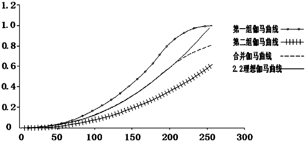
[0057] Please refer to Figure 5 , Figure 5 This is the work flow chart of the perspective switching architecture of the third embodiment. The viewing angle switching method provided by this embodiment is basically the same as the second embodiment, except that: the first polarity control signal is a fixed voltage signal; the multiple external supply voltages are multiple first gamma voltages; the second polarity The control signal is an inverted signal per frame;
[0058] Wherein, the step of resetting according to the reset signal and periodically outputting the second group of gamma voltages and the third group of gamma voltages according to the second polarity control signal cycle includes: the first processing module stores the second voltage generation instruction and the first Three voltage generation instructions, according to the second polarity control signal to alternately execute the second voltage generation instruction and the third voltage generation instruction to alternately output the second group of gamma voltages and the third group of gamma voltages.
[0059] Specifically, this embodiment provides a method for switching perspective switching architecture, such as Figure 5 As shown, including the following steps:
[0060] S21: The timing control module determines whether the mode control signal is the first display mode control signal or the second display mode control signal;
[0061] S22: The timing control module outputs a voltage calling instruction and a first polarity control signal according to the first display mode control signal, where the first polarity control signal is a fixed voltage signal;
[0062] S23: The first processing module outputs a first voltage generation instruction according to the first display mode control signal;
[0063] S24. The second processing module receives the first polarity control signal and the first voltage generation instruction, and executes the first voltage generation instruction to output multiple external supply voltages, where the multiple external supply voltages are multiple first gamma voltages;
[0064] S25: The source driving module receives a voltage call instruction, uses an internal gamma correction circuit, and receives multiple external supply voltages to obtain a first group of gamma voltages;
[0065] Wherein, all the first gamma voltages in the first group of gamma voltages may be part or all of multiple external supply voltages;
[0066] S26: The timing control module outputs a second polarity control signal according to the second display mode control signal, where the second polarity control signal is an inversion signal per frame;
[0067] S27: The first processing module outputs a reset signal according to the second display mode control signal;
[0068] S28. The second processing module resets according to the reset signal, and executes the second voltage generation command and the third voltage generation command alternately according to the second polarity control signal cycle to alternately output the second group of gamma voltages and the third group Gamma voltage
[0069] S29: The source driving module drives and outputs pixel signals according to the first group of gamma voltages, the second group of gamma voltages or the third group of gamma voltages.
[0070] For the specific implementation of this implementation, reference may be made to the first embodiment, which will not be repeated here.
[0071] The viewing angle switching method of this embodiment can support three sets of gamma voltages, and supports the switching use of two sets of gamma voltages in one display mode, thereby effectively improving the image quality of the display screen of the liquid crystal display device.

PUM

no PUM

Description & Claims & Application Information

We can also present the details of the Description, Claims and Application information to help users get a comprehensive understanding of the technical details of the patent, such as background art, summary of invention, brief description of drawings, description of embodiments, and other original content. On the other hand, users can also determine the specific scope of protection of the technology through the list of claims; as well as understand the changes in the life cycle of the technology with the presentation of the patent timeline. Login to view more.

Similar technology patents

Oil-based ink composition for ink-jet recording

InactiveCN101225268AImprove picture qualityExcellent image fixationInksPrintingEmulsionDiol
Owner:SEIKO EPSON CORP

Classification and recommendation of technical efficacy words

Why Eureka
Try Eureka