
Photo-thermal effect simulation method for a surface plasmon waveguide

A surface plasmon and plasmon waveguide technology, applied in design optimization/simulation, special data processing applications, instruments, etc., can solve low efficiency, high cost, and inability to obtain the distribution of optical and thermal fields, etc. problem, to achieve the effect of accurate results, high simulation efficiency and wide application range

Active Publication Date: 2019-03-19
NANJING UNIV OF POSTS & TELECOMM
View PDF4 Cites 3 Cited by
  • Summary
  • Abstract
  • Description
  • Claims
  • Application Information

AI Technical Summary

Problems solved by technology

[0004] Using experiments to study the photothermal effect of surface plasmon waveguides is not only expensive but also inefficient. playing an increasingly important role in
The actual surface plasmon waveguide usually has a three-dimensional complex structure, and the two-dimensional approximation method cannot obtain accurate results well, and the traditional analytical method cannot obtain the distribution of the optical and thermal fields

Method used


Image

  • Photo-thermal effect simulation method for a surface plasmon waveguide
  • Photo-thermal effect simulation method for a surface plasmon waveguide
  • Photo-thermal effect simulation method for a surface plasmon waveguide

Examples


Embodiment Construction

[0037] The technical solutions of the present invention will be further described below in conjunction with the accompanying drawings and embodiments.

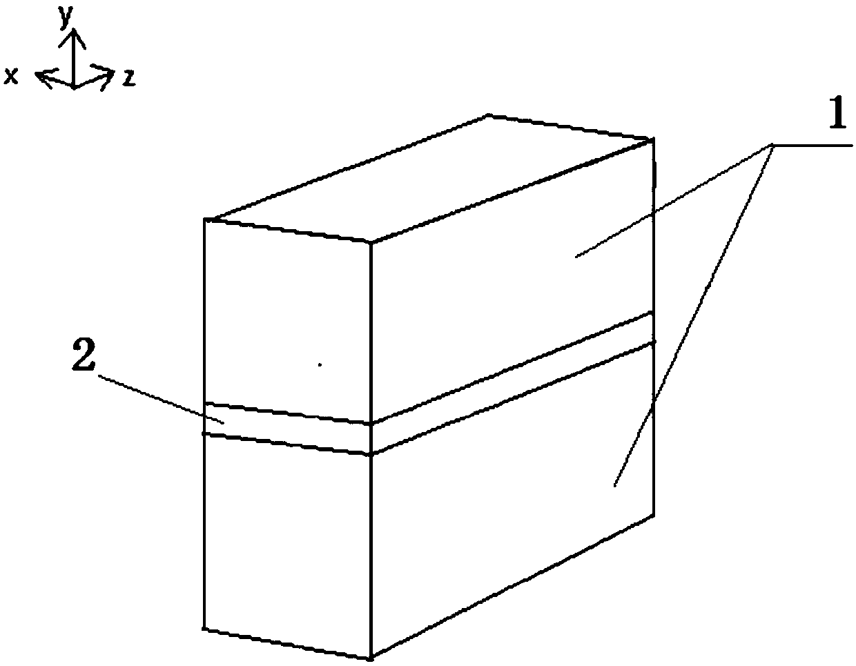
[0038] like figure 1 The main flow of the photothermal effect simulation method of the surface plasmon waveguide described in the present invention is shown, including the following steps:

[0039] S1: Construct the simulation area of ​​the three-dimensional surface plasmon waveguide, and use the vector wave equation of the electric field as the control equation in the light simulation area,

[0040]

[0041] where μ r is the relative magnetic permeability, E is the total electric field, k 0 is the wave number, ε r is the relative permittivity.

[0042] The perfect matching layer is used to truncate the light simulation area as the boundary of the simulation area, and the Dirichlet boundary condition is used outside the perfect matching layer to impose the electric field value as 0 as the boundary condition, so as to ob...


PUM


Abstract

The invention discloses a photo-thermal effect simulation method for a surface plasmon waveguide. The method comprises the following steps: firstly, determining an edge value problem of a light fieldpart based on an electric field vector wave equation and an electromagnetic boundary condition, discretizing a light field analysis area by adopting tetrahedral vector edge elements, establishing a light field finite element matrix equation according to a Galerkin method, and solving to obtain electric field distribution of a three-dimensional surface plasmon waveguide; then, heat generated by anelectric field is used as a heat source; determining an edge value problem of a thermal field part based on a transient heat conduction equation and a thermal boundary condition; a tetrahedral scalarnode element is adopted to discretize a thermal field analysis area, an unconditionally stable backward difference format is adopted to discretize a time domain, a thermal field finite element matrixequation of each time step is established according to a Galerkin method, and transient temperature distribution of the three-dimensional surface plasmon waveguide is obtained through solving. The method has the advantages of being high in simulation precision, wide in application range and high in solving efficiency.

Description

technical field [0001] The invention relates to a surface plasmon simulation method, in particular to a three-dimensional numerical simulation method of the photothermal effect of a surface plasmon waveguide. Background technique [0002] The integrated optical circuit is composed of tiny photonic devices. However, because the size of photonic devices is limited by the diffraction limit, it is difficult to nanometerize and integrate them. The use of surface plasmons can break through the diffraction limit, thereby realizing the nanometerization and integration of photonic devices. A surface plasmon is a surface electromagnetic wave mode propagating at the interface of two media with opposite permittivity signs. Due to its surface-wave properties, beams can be confined to the subwavelength scale. Therefore, optical waveguides based on surface plasmons, that is, surface plasmon waveguides, have great potential in fabricating highly integrated photonic chips. [0003] When l...

Claims


Application Information

Patent Timeline
Patent Type & Authority Applications(China)
IPC IPC(8): G06F17/50
CPCG06F30/23Y02E60/00
Inventor 宛汀郭宇翔唐奔流张贵成
Owner NANJING UNIV OF POSTS & TELECOMM
Learn More