Semiconductor element with double-sided heat conduction and heat radiation structure

A heat dissipation structure and semiconductor technology, applied in the direction of semiconductor devices, semiconductor/solid-state device components, electrical components, etc., can solve the problems of poor heat conduction and heat dissipation, and achieve the effect of prolonging the service life, improving the use effect, and improving the heat dissipation effect.

Pending Publication Date: 2019-03-19
深圳市元拓高科半导体有限公司
View PDF0 Cites 1 Cited by
  • Summary
  • Abstract
  • Description
  • Claims
  • Application Information

AI Technical Summary

Problems solved by technology

[0004] The object of the present invention is to provide a semiconductor element with a double-sided heat conduction and heat dissipation structure, so as to solve the problem of poor heat conduction and heat dissipation effect of semiconductor devices existing in the prior art

Method used


Image

  • Semiconductor element with double-sided heat conduction and heat radiation structure
  • Semiconductor element with double-sided heat conduction and heat radiation structure
  • Semiconductor element with double-sided heat conduction and heat radiation structure

Examples


Embodiment 1

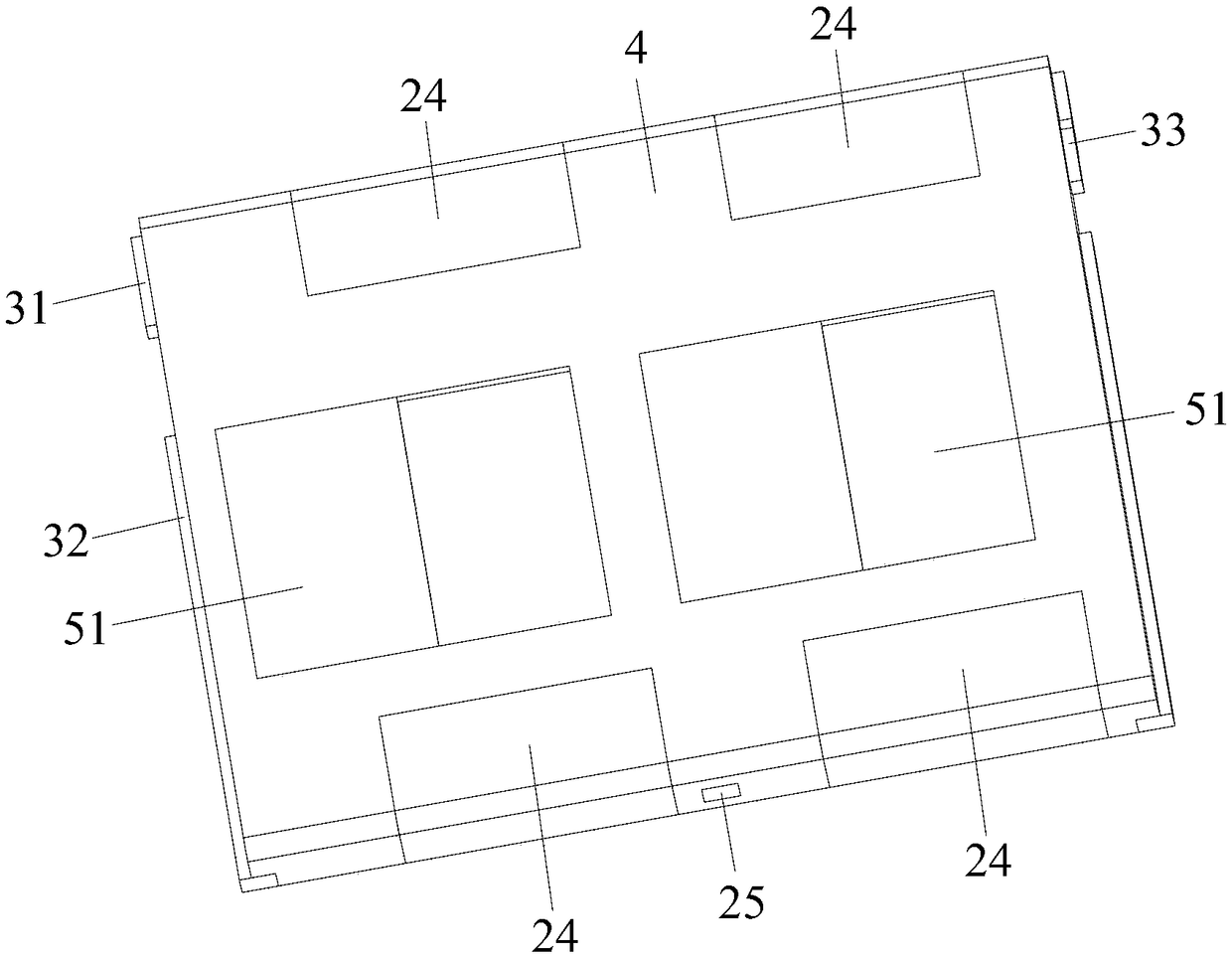
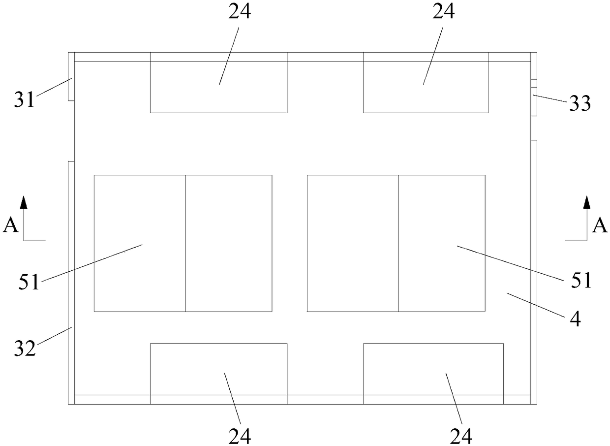
[0043] Please also refer to Figure 1 to Figure 11Now, the semiconductor element with double-sided heat conduction and heat dissipation structure provided by Embodiment 1 of the present invention will be described. The semiconductor element includes a substrate 2, a chip 1 disposed on the substrate 2, a pin 3 electrically connected to the chip 1 through a conductor 6, and an adhesive fixed and molded on the substrate 2 to seal and fix the chip 1 and the pin 3. Seat 4. A window 40 is provided on the rubber base 4 corresponding to the position of the chip 1. The semiconductor element also includes a heat conduction and heat dissipation plate 51 arranged in the window 40. The window 40 can wrap and fix the periphery of the heat conduction and heat dissipation plate 51. The chip 1 Located between the heat conduction plate 51 and the substrate 2 , the top surface of the chip 1 is attached to the bottom surface of the heat conduction plate 51 , and the bottom surface of the chip 1 ...

Embodiment 2

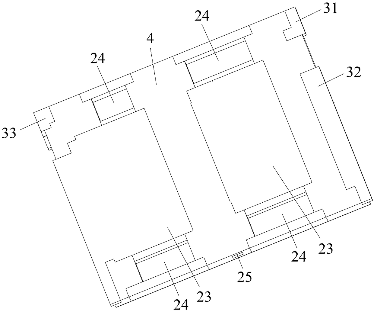
[0075] Please also refer to Figure 12 with Figure 13 Now, the semiconductor element with double-sided heat conduction and heat dissipation structure provided by Embodiment 2 of the present invention will be described. The difference between this embodiment two and the above-mentioned embodiment one is:

[0076] 1. Cancel the heat conduction and heat dissipation plate 51, simplify the production process and reduce the cost;

[0077] 2. The front side of the semiconductor element of the first embodiment is used as the back side of the semiconductor element of the second embodiment, and the back side of the semiconductor element of the first embodiment is used as the front side of the semiconductor element of the second embodiment;

[0078] 3. The connection board 24 is on the same plane as the pins 3 .


PUM


Abstract

The invention is applicable to the technical field of electronic equipment, and provides a semiconductor element with a double-sided heat conduction and heat radiation structure. The semiconductor element with a double-sided heat conduction and heat radiation structure comprises a substrate, a chip, a conductor with one end connected with the chip, a pin connected with the other end of the conductor, a rubber seat and a heat conduction and heat radiation plate, wherein a window is opened in the rubber seat; one end of the heat conduction and heat radiation plate is fit with the chip and the other end reaches out of the chip. As the window is arranged at the position, corresponding to the chip, on the rubber seat, the window is provided with the heat conduction and heat radiation plate fitwith the chip, and one surface of the chip can be fit with the heat conduction and heat radiation plate and the other surface can be fit with the substrate, the heat of the chip can be transferred tothe substrate and the heat conduction and heat radiation plate respectively and is diffused, the semiconductor element can diffuse the heat of the chip at two sides, and the heat radiation effects ofthe semiconductor element can further be improved; and the chip and the pin are connected through the conductor, the conductor can also transfer part of the heat of the chip to the pin and diffuse theheat, and thus, the heat radiation effects are further improved.

Description

technical field [0001] The invention is applicable to the technical field of electronic equipment, and more specifically relates to a semiconductor element with a double-sided heat conduction and heat dissipation structure. Background technique [0002] A semiconductor device refers to an object whose conductivity is between a conductor and an insulator at room temperature. Because its conductivity can be controlled, ranging from an insulator to a conductor, it is widely used in the technical field of electronic equipment. [0003] Existing semiconductor devices mainly transfer heat to a PCB (Printed Circuit Board, printed circuit board) bonded thereto through the metal sheet attached to the chip, and then transfer the heat to peripheral components to achieve heat dissipation. Since the semiconductor device can only realize one-sided heat dissipation, the heat dissipation effect of the semiconductor device is poor, which will affect the working performance and efficiency of ...

Claims


Application Information

Patent Timeline
Patent Type & Authority Applications(China)
IPC IPC(8): H01L23/047H01L23/367H01L23/49
CPCH01L23/047H01L23/3672H01L23/49
Inventor 伍昭云郭正谡
Owner 深圳市元拓高科半导体有限公司
Why Eureka
Try Eureka