A kind of circuit board electroplating process method

An electroplating process and circuit board technology, applied in the directions of printed circuits, electrical components, printed circuit manufacturing, etc., can solve the problems of different electroplating current density, uneven electroplating thickness, thick electroplating thickness, etc., to achieve low implementation cost and improve electroplating uniformity. sexual effect

An electroplating process and circuit board technology, applied in the directions of printed circuits, electrical components, printed circuit manufacturing, etc., can solve the problems of different electroplating current density, uneven electroplating thickness, thick electroplating thickness, etc., to achieve low implementation cost and improve electroplating uniformity. sexual effect

CN109496080BActive Publication Date: 2021-04-09JCET GROUP CO LTD

Image

  • A kind of circuit board electroplating process method
  • A kind of circuit board electroplating process method
  • A kind of circuit board electroplating process method

Examples


Embodiment Construction

[0030]The present invention will be further described in detail below with reference to the accompanying drawings embodiments.

[0031]One type of circuit board in this embodiment includes the following steps:

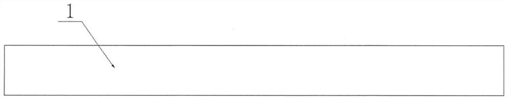
[0032]Step one, seefigure 1 , Take a metal substrate, a metal substrate surface pre-copper;

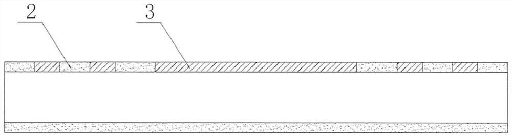
[0033]Step 2, seefigure 2 In the surface of the metal substrate, the photoresist film is subjected to exposure, and the photoresist film is exposed, and the positive surface of the metal substrate is subsequently required, and the first line layer is formed by electroplating in the pattern area;

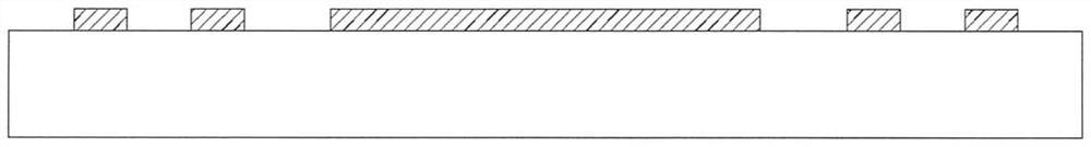
[0034]Step three, seeimage 3 , Remove the photoresist film;

[0035]Step four, seeFigure 4 In the front surface of the metal substrate, the ABF film is pressed, and the thermosetting operation is carried out, and the first line layer is covered into the Curing ABF film;

[0036]Step 5, seeFigure 5 , Reduce the first line layer to expose the ABF film;

[0037]Step six, seeFigure 6 , In the surface of the metal ...


PUM


Abstract

The invention relates to a circuit board electroplating process, which comprises the following steps: step 1, taking a metal substrate; step 2, electroplating the first circuit layer on the front of the metal substrate; step 3, pressing an ABF film on the front of the metal substrate, and heat Curing operation, so that the first metal layer is coated in the cured ABF film; step 4, thinning the first metal layer to expose the ABF film; step 5, electroplating on the front of the metal substrate to form the second circuit layer, and on the back of the metal substrate Electroplating forms a compensation circuit layer; Step 7, removing the remaining photoresist film; Step 8, window etching; a circuit board electroplating process method of the present invention, which optimizes the thickness of the front electroplating by designing the compensation area on the back of the carrier board, and improves the overall layout of the circuit. Uniformity of plating.

Description

Technical field[0001]The present invention relates to a circuit board electroplating process, which belongs to the technical field of precision circuit board.Background technique[0002]With the diversification, miniaturization of the electronic product, the precision level of the circuit board is increasing, and in conventional plating lines, due to different electroplating line distributions, the electroplating current density is different, and the current density is small when the excessive plating line is electroplated. Thick thickness, large current density is thick thick, so it is easy to generate uneven electroplating thickness, osmium plating, and clipping. The line distribution is generally electrically demanding, it is difficult to solve these problems by design optimization, while light from improving electroplating process capabilities, and the investment cost is relatively high.Inventive content[0003]The technical problem to be solved by the present invention is to provid...

Claims


Application Information

Patent Timeline
09 Apr 2021
Publication
CN109496080B
IPC
H05K3/18; H05K3/00
CPC
H05K3/0005; H05K3/18
Inventors
吴昊平; 张江华