Method of filling groove structure with tungsten
A metal structure, tungsten layer technology, applied in electrical components, semiconductor/solid state device manufacturing, circuits, etc., can solve the problems affecting the performance of tungsten metal structure, unfavorable filling grooves, etc., to improve filling quality, improve aspect ratio, The effect of increasing the aspect ratio
- Summary
- Abstract
- Description
- Claims
- Application Information
AI Technical Summary
Problems solved by technology
Method used
Image
Examples
Embodiment Construction
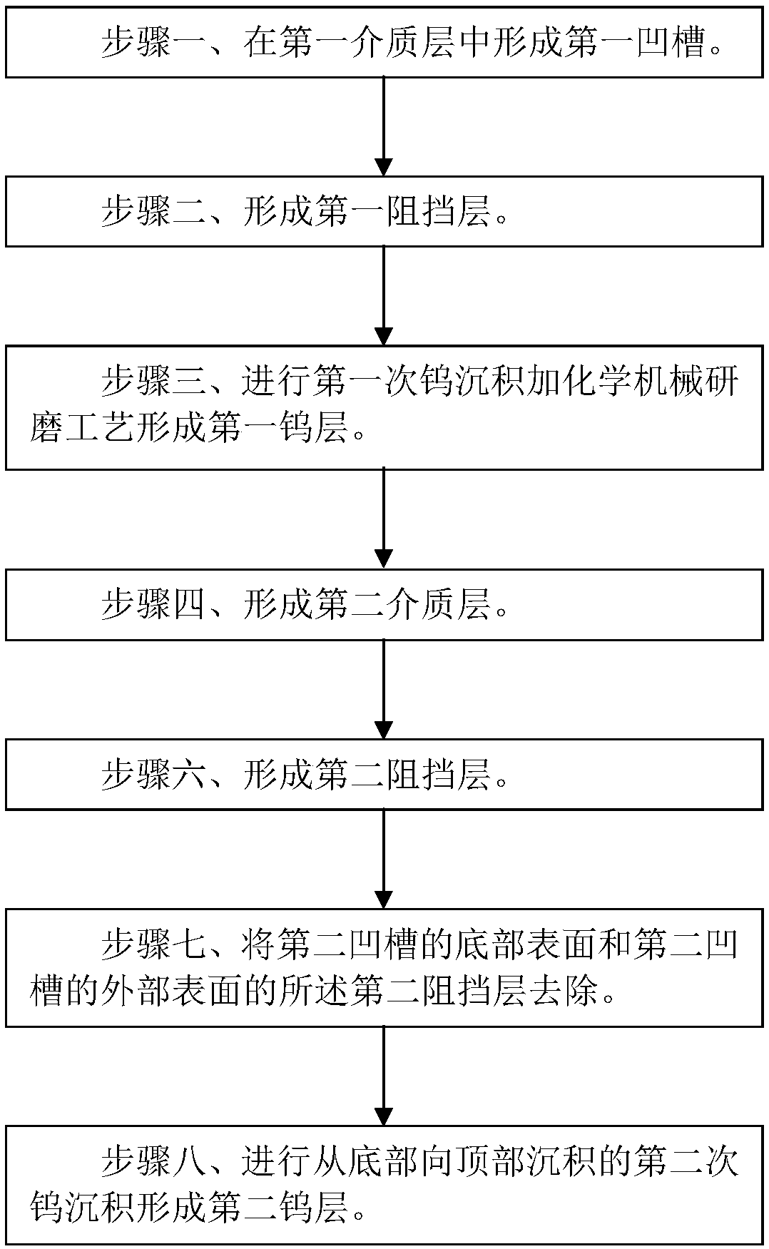
[0035] Such as figure 1 Shown is the flowchart of the method for filling the groove structure with tungsten in the embodiment of the present invention; as Figure 2A to Figure 2I As shown, it is a device structure diagram in each step of the method of the embodiment of the present invention. The method for filling the groove structure with tungsten in the embodiment of the present invention includes the following steps:
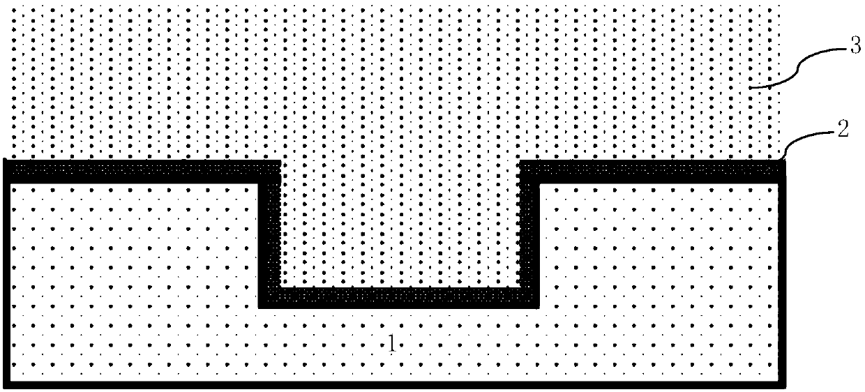
[0036] Step 1, such as Figure 2A As shown, a first groove 101 is formed in the first dielectric layer 1 .
[0037] The depth of the first groove 101 is less than 1 / 3 of the depth of the subsequently formed second groove 102 .
[0038] Step two, such as Figure 2A As shown, a first barrier layer 2 is formed, and the first barrier layer 2 is formed on the bottom surface and side surfaces of the first groove 101 and extends to the surface outside the first groove 101 .
[0039] The first barrier layer 2 is a stacked layer of Ti and TiN.
[0040] Step three...
PUM
 Abstract
Description
Claims
Application Information


