Production method of phase-change memory

A technology of phase change memory and manufacturing method, which is applied in the field of phase change memory, and can solve problems such as difficulty in achieving uniform coverage of metal seed layers, poor filling ability of small holes, poor electroplating results, etc., and achieve good filling quality of small holes , low cost and simple method

Inactive Publication Date: 2010-09-08
INST OF SEMICONDUCTORS - CHINESE ACAD OF SCI
View PDF5 Cites 8 Cited by
  • Summary
  • Abstract
  • Description
  • Claims
  • Application Information

AI Technical Summary

Problems solved by technology

[0004] At present, the methods for filling small holes mainly include magnetron sputtering, electroplating, CVD, etc., but they have some shortcomings more or less, such as the small hole filling ability of magnetron sputtering and other sputtering methods is not strong, CVD method The cost is high; although the electroplating method is low in cost, it needs to use the sputtering method to prepare a layer of metal seed layer first, and when the aperture of the small hole is reduced to a certain scale, the metal seed layer prepared by sputtering is difficult to achieve uniform coverage, which will lead to Poor plating results

Method used


Image

  • Production method of phase-change memory
  • Production method of phase-change memory
  • Production method of phase-change memory

Examples


Embodiment Construction

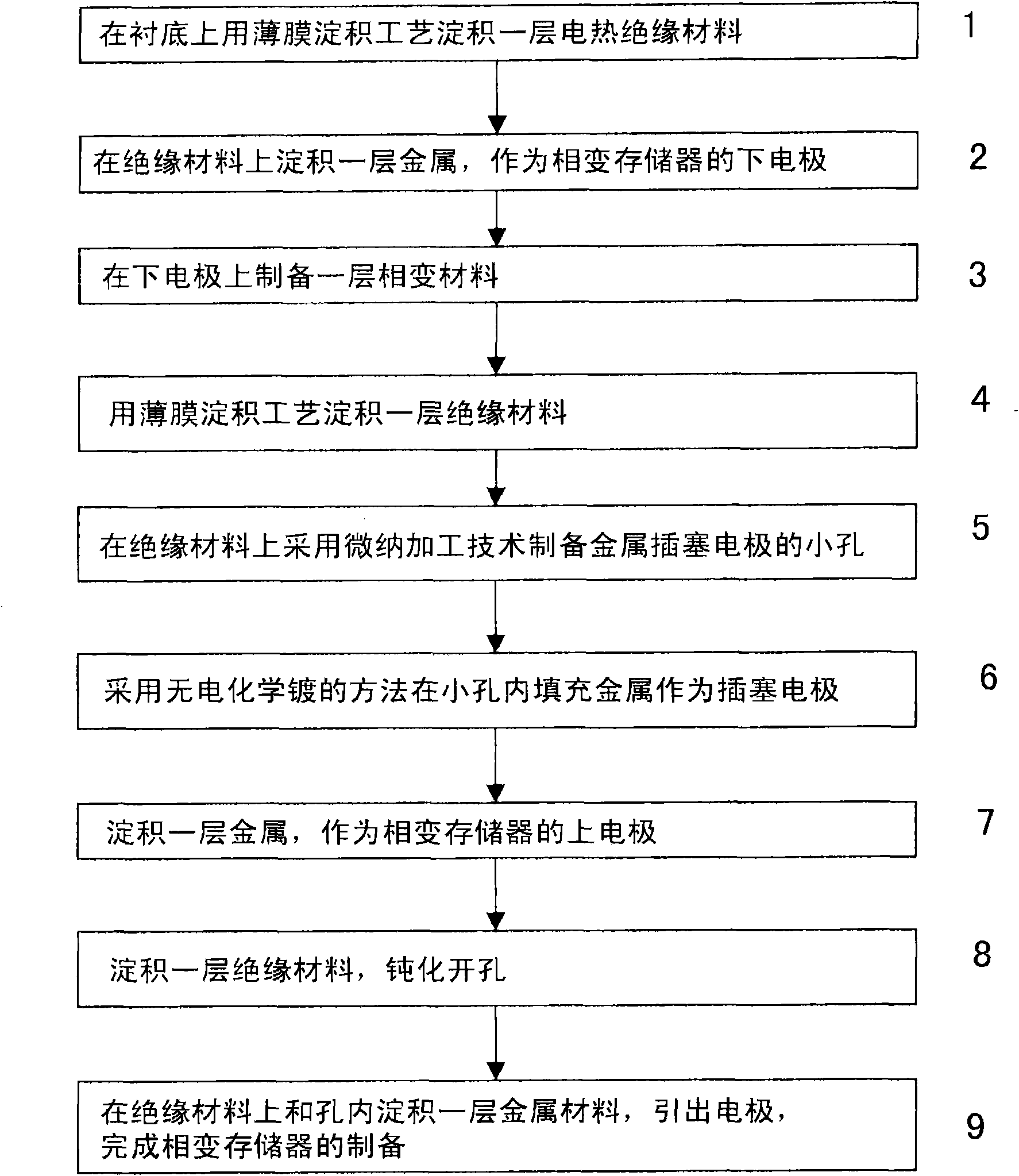
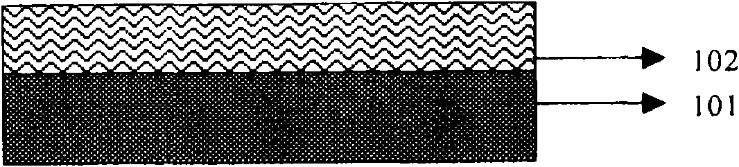
[0029] see Figure 1 to Figure 10 As shown, the present invention introduces a preparation method of a phase change memory, comprising the following steps:

[0030] Step 1: Deposit a layer of first insulating material layer 102 on the substrate 101 . The substrate 101 is a semiconductor material substrate silicon wafer, or a substrate including a phase-change memory drive circuit; the first insulating material layer 102 can be oxide, nitride, sulfide or oxide Any one of a mixture of at least two of , nitride, and sulfide; the first insulating material layer 102 grown on the substrate can be sputtered, evaporated, or plasma-assisted deposition method, chemical vapor deposition method, metal-organic compound thermal decomposition method, laser-assisted deposition method and thermal oxidation method (such as figure 2 shown);

[0031] Step 2: Deposit a layer of metal layer 103 on the first insulating material layer 102 as the lower electrode of the phase change memory; the met...


PUM

PropertyMeasurementUnit
diameteraaaaaaaaaa

Abstract

The invention relates to a production method a phase-change memory, which comprises the following steps: step 1, depositing a first insulating material layer on a substrate; step 2, depositing a metal layer on the first insulating material layer to be used as a lower electrode of the phase-change memory; step 3, preparing a phase-change material layer on the metal layer; step 4, depositing a second insulating material layer on the phase-change material layer by a thin film deposition process; step 5, preparing small holes of metal plug electrodes on the second insulating material layer by micro/nano processing technology; step 6, filling metal in the small holes to be used as plug electrodes by adopting a non-electrochemical plating method; step 7, depositing a metal material layer on the second insulating material layer to be used as an upper electrode of the phase-change memory; step 8, depositing a third insulating material layer on the metal material; step 9, carrying out passivation opening on the third insulating material layer; and step 10: depositing a metal electrode layer on the third insulating material layer and in the passivation opening again to complete the production of the phase-change memory.

Description

technical field [0001] The present invention relates to the field of microelectronics manufacturing technology, in particular to a method for manufacturing a phase-change memory, which avoids the defects of poor filling quality and high cost of small hole filling in traditional small hole filling methods such as sputtering, electroplating, and CVD. Traditional metal plug electrodes have great advantages in terms of high preparation cost, complex process limitations, and improvement of storage density and device performance of phase change memory. Background technique [0002] Phase change memory PRAM (phase change random access memory, PRAM) is a new semiconductor memory, compared with the existing semiconductor storage technology, including conventional volatile technology and non-volatile technology, has the Small size, low power consumption, multi-level storage, long cycle life, high-speed reading, anti-radiation, high and low temperature resistance, anti-electronic inter...

Claims


Application Information

Patent Timeline
Patent Type & Authority Applications(China)
IPC IPC(8): H01L45/00H01L21/768
Inventor 马慧莉王晓峰王晓东杨富华
Owner INST OF SEMICONDUCTORS - CHINESE ACAD OF SCI
Why Eureka
Try Eureka