Method for achieving through hole interconnection by filling through hole from bottom to top and product thereof

A bottom-up, product technology, applied in the direction of semiconductor/solid-state device components, semiconductor devices, electrical components, etc., can solve the problems of long process flow and low efficiency, and achieve the goal of simplifying process steps, facilitating control, and improving electroplating efficiency. Effect

Inactive Publication Date: 2013-09-25
HUAZHONG UNIV OF SCI & TECH
View PDF3 Cites 8 Cited by
  • Summary
  • Abstract
  • Description
  • Claims
  • Application Information

AI Technical Summary

Problems solved by technology

However, the production of the seed layer in this method generally requires additional process steps, such as making auxiliary wafers and temporary bonding of the auxiliary wafers; or it is necessary to pre-fill the seed layer and electroplating on the back of the wafer to be plated; therefore, there is a long process flow and high efficiency. Defects such as inferiority

Method used


Image

  • Method for achieving through hole interconnection by filling through hole from bottom to top and product thereof
  • Method for achieving through hole interconnection by filling through hole from bottom to top and product thereof
  • Method for achieving through hole interconnection by filling through hole from bottom to top and product thereof

Examples


Embodiment Construction

[0041] In order to make the object, technical solution and advantages of the present invention clearer, the present invention will be further described in detail below in conjunction with the accompanying drawings and embodiments. It should be understood that the specific embodiments described here are only used to explain the present invention, not to limit the present invention. In addition, the technical features involved in the various embodiments of the present invention described below can be combined with each other as long as they do not constitute a conflict with each other.

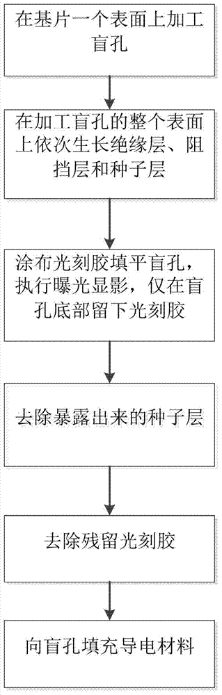
[0042] figure 1 It is a schematic diagram of the technological process of realizing through-hole interconnection through bottom-up filling according to the present invention. like figure 1 As shown in, the method for realizing via interconnection according to the present invention mainly includes the following steps:

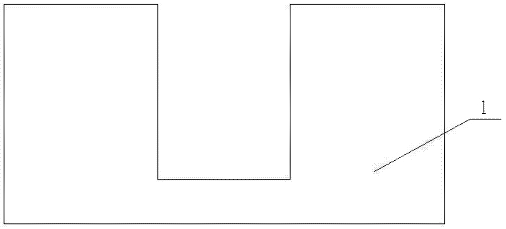
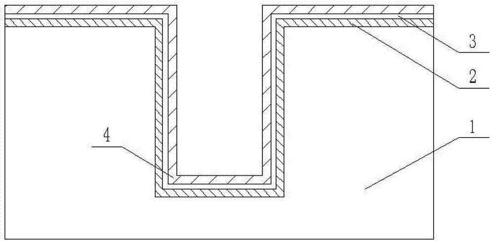
[0043] First, refer to Figure 2a As shown in , a blind hole is processed o...


PUM

PropertyMeasurementUnit
thicknessaaaaaaaaaa

Abstract

The invention discloses a method for achieving through hole interconnection by filling a through hole from bottom to top. The method includes the steps that (a) a blind hole is machined in one surface of a substrate; (b) an insulating layer, a barrier layer and a seed layer are sequentially formed on the surface, provided with the blind hole, of the substrate; (c) the surface of the seed layer is coated with photoresist, the blind hole is filled and leveled up, and then exposure and development treatment is carried out so that the photoresist can only remain on the portion, at the bottom of the blind hole, of the surface of the seed layer; (d) the portion, not covered with the photoresist, of the seed layer is removed, wherein the portion, at the bottom of the blind hole, of the seed layer is not affected; (e) the residual photoresist is removed; (f) conducting materials are filled into the blind hole to achieve generation from bottom to top; (g) the surface, not provided with the blind hole, of the substrate is thinned so that a through hole can be formed, and then the process of through hole interconnection is finished. The invention further discloses a corresponding through hole interconnection structure product. By means of the method, the process of through hole electroplating can be carried out with convenient control, low cost and high efficiency, and the through hole interconnection structure product with better filling effects can be obtained.

Description

technical field [0001] The invention belongs to the technical field of semiconductor packaging, and more specifically relates to a method for realizing through-hole interconnection through bottom-up filling and a product thereof. Background technique [0002] In the past few decades, integrated circuit technology has maintained a high-speed development following Moore's Law, the performance of chips has been greatly improved, power consumption and cost have also been greatly reduced, but the development of electronic packaging technology is relatively slow. , has gradually become one of the bottlenecks restricting the development of semiconductor technology. The traditional two-dimensional integration form has been unable to meet the increasingly higher requirements for the speed and volume of integrated circuits in consumer electronics, aerospace and other industries. Therefore, three-dimensional integration technology is receiving more and more attention. much attention an...

Claims


Application Information

Patent Timeline
Patent Type & Authority Applications(China)
IPC IPC(8): H01L21/60H01L21/288H01L21/74H01L23/528H01L23/532
Inventor 廖广兰薛栋民史铁林宿磊独莉张昆
Owner HUAZHONG UNIV OF SCI & TECH
Why Eureka
Try Eureka