
Solid-state imaging device, method for driving solid-state imaging device, and electronic apparatus

A solid-state imaging device and electric charge technology, which is applied in television, electrical components, image communication, etc., can solve problems such as the inability to realize global shutter readout, achieve wide dynamic range, expand effective pixel area, and increase value.

Active Publication Date: 2019-04-02
PRILUNICUS SINGAPORE PTE LTD
View PDF16 Cites 4 Cited by
  • Summary
  • Abstract
  • Description
  • Claims
  • Application Information

AI Technical Summary

Problems solved by technology

[0010] However, this type of MOS image sensor has the disadvantage of being unable to realize global shutter readout, although it is capable of high-speed signal transmission.

Method used


Image

  • Solid-state imaging device, method for driving solid-state imaging device, and electronic apparatus
  • Solid-state imaging device, method for driving solid-state imaging device, and electronic apparatus
  • Solid-state imaging device, method for driving solid-state imaging device, and electronic apparatus

Examples


no. 1 approach

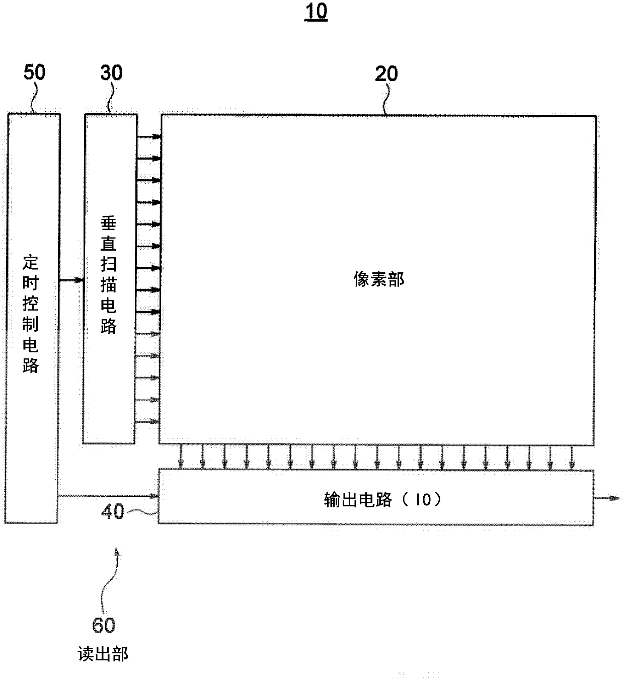
[0067] figure 1 It is a block diagram showing a configuration example of the solid-state imaging device according to the first embodiment of the present invention.

[0068] In the present embodiment, the solid-state imaging device 10 is constituted by, for example, a CMOS image sensor including digital pixels (Digital Pixels) as pixels.

[0069] Such as figure 1 As shown, the solid-state imaging device 10 has a pixel unit 20 as an imaging unit, a vertical scanning circuit (row scanning circuit) 30 , an output circuit 40 , and a timing control circuit 50 as main components.

[0070] Among these components, for example, the vertical scanning circuit 30 , the output circuit 40 , and the timing control circuit 50 constitute a pixel signal readout unit 60 .

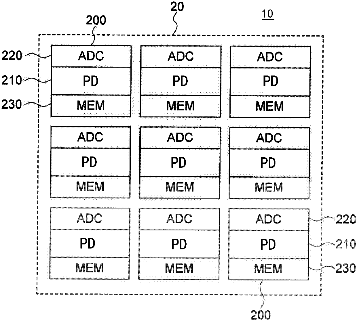
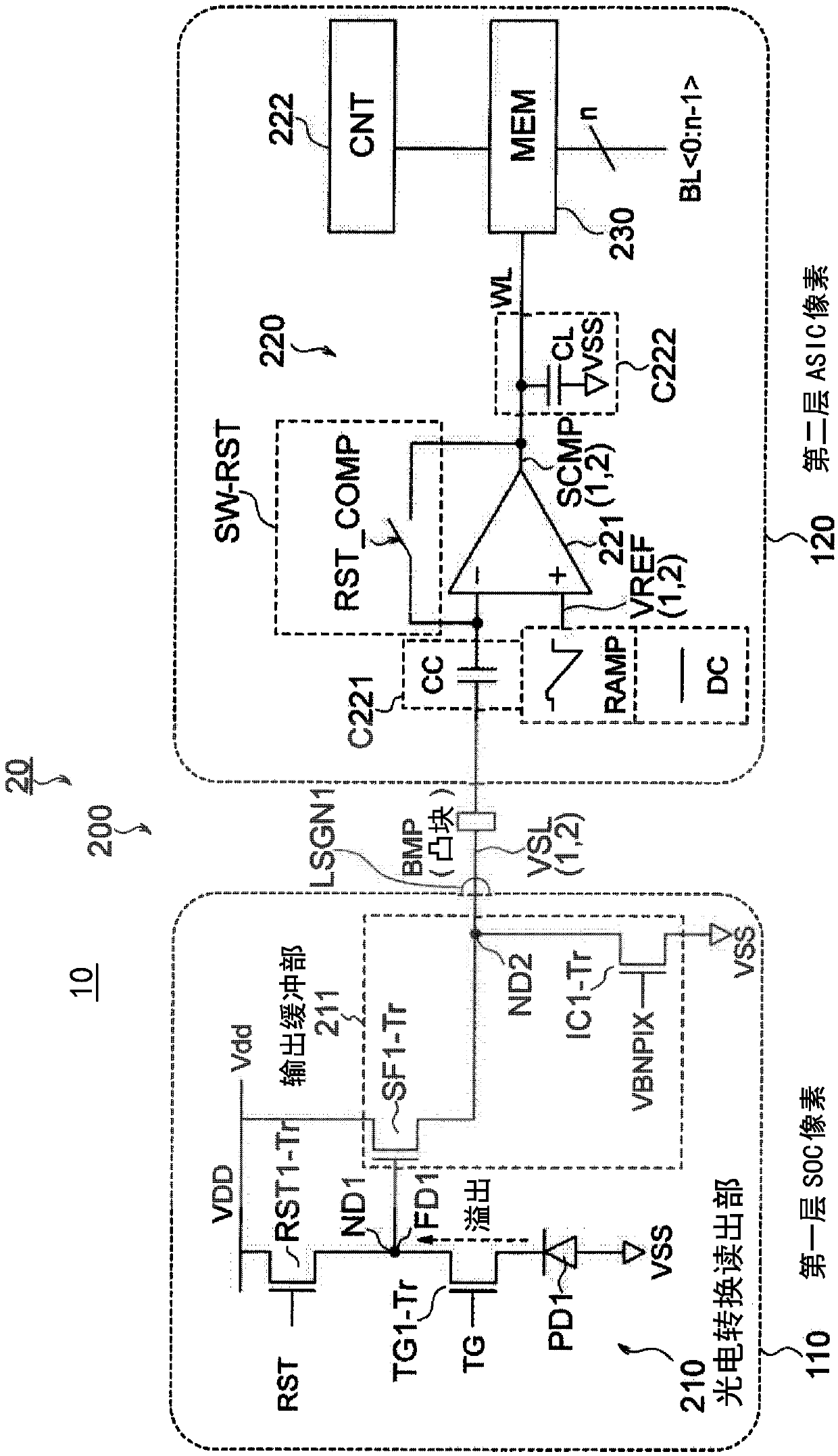
[0071] In the first embodiment, the solid-state imaging device 10 includes a photoelectric conversion readout unit, an AD (analog-to-digital) conversion unit, and a memory unit as digital pixels in the pixel unit 20, and is ...

no. 2 approach

[0251] Figure 15 It is a diagram for explaining the solid-state imaging device according to the second embodiment of the present invention, and is a diagram showing an example of selection processing between the time stamp ADC mode operation and the linear ADC mode operation.

[0252] The difference between the solid-state imaging device 10A of the second embodiment and the solid-state imaging device 10 of the first embodiment described above is as follows.

[0253] In the solid-state imaging device 10 of the first embodiment, the time stamp (TS) ADC mode operation and the linear (Lin) ADC mode operation are continuously performed.

[0254] In contrast, in the solid-state imaging device 10A according to the second embodiment, it is possible to selectively perform time stamp (TS) ADC mode operation and linear (Lin) ADC mode operation according to illuminance.

[0255] exist Figure 15 In the example of , when the illuminance is normal ( ST1 ), the time stamp ADC mode operati...

no. 3 approach

[0260] Figure 16 It is a diagram showing an example of frame readout timing in the solid-state imaging device 10B according to the third embodiment of the present invention. exist Figure 16 , TS shows the timestamp ADC.

[0261] Figure 17 It is a diagram showing the state of optical time conversion when a reference voltage is input to the comparator of the third embodiment.

[0262] exist Figure 17 , shows a time example of the inversion timing (ramp reference voltage), the horizontal axis shows the sampling time, and the vertical axis shows the estimated signal in the overflow signal. Here, the overflow signal refers to a signal estimated under the condition (non-overflow) that charges are not accumulated in the photodiode PD1 when the transfer transistor TG1-Tr is turned on.

[0263] Figure 17 The sampling time of the comparator 221 inversion corresponding to the non-overflow charge (signal) based on the property (adaptability) of the applied light is shown.

[0...


PUM


Abstract

A Solid-state imaging device, A method for driving THE solid-state imaging device, and an electronic apparatus are provided. An AD conversion part (220) has a comparator (221) for performing comparison processing comparing a voltage signal read out by a photoelectric converting and reading part (210) and a reference voltage and outputting a digitalized comparison result signal, the comparator (221), under the control by a reading part (60), performs first comparison processing for outputting a digitalized first comparison result signal with respect to a voltage signal corresponding to an overflow charge overflowing from a photodiode (PD1) to a floating diffusion (FD1) in an integration period and second comparison processing for outputting a digitalized second comparison result signal withrespect to a voltage signal corresponding to an accumulated charge of the photodiode (PD1) transferred to the floating diffusion (FD1) in a transfer period after the integration period. Due to this,it becomes possible to substantially realize a broader dynamic range and a higher frame rate.

Description

[0001] Citations for Associated Applications [0002] The present application contains subject matter related to Japanese Patent Applications JP2017-185502 and JP2017-185504 filed in the Japan Patent Office on Sep. 26, 2017, the entire contents of which are incorporated herein by reference. technical field [0003] The present invention relates to a solid-state imaging device, a driving method of the solid-state imaging device, and electronic equipment. Background technique [0004] As a solid-state imaging device (image sensor) using a photoelectric conversion element that detects light and generates charges, a CMOS (Complementary Metal Oxide Semiconductor) image sensor is actually used. [0005] CMOS image sensors are widely used as part of various electronic devices such as digital cameras, video cameras, surveillance cameras, medical endoscopes, personal computers (PCs), and mobile phones. [0006] The CMOS image sensor has an FD amplifier for each pixel. The FD amplifi...

Claims


Application Information

Patent Timeline
Patent Type & Authority Applications(China)
IPC IPC(8): H04N5/374H04N5/3745H04N5/378H04N5/355H04N5/357H04N5/361
CPCH04N25/59H04N25/60H04N25/63H04N25/76H04N25/77H04N25/75H03M1/56H03M1/123H03M1/0607H04N25/575H04N25/772H04N25/79H04N25/767H04N25/40H04N25/587
Inventor 盛一也大高俊德高柳功中村淳一安田直人
Owner PRILUNICUS SINGAPORE PTE LTD
Learn More