Substrate detection system and substrate detection method

A substrate detection and substrate technology, which is applied in measuring devices, optical testing of flaws/defects, and material analysis through optical means, can solve problems such as time-consuming, difficult, and impossible to trace and find the cause of glass substrate fragmentation, and achieve The effect of improving yield rate, reducing production cost, and improving process yield rate

Inactive Publication Date: 2019-04-05
WUHAN CHINA STAR OPTOELECTRONICS SEMICON DISPLAY TECH CO LTD
View PDF9 Cites 0 Cited by
  • Summary
  • Abstract
  • Description
  • Claims
  • Application Information

AI Technical Summary

Problems solved by technology

In particular, when the glass substrate is broken in the stripping machine or the back-end process, it is impossible to trace and find

Method used


Image

  • Substrate detection system and substrate detection method
  • Substrate detection system and substrate detection method
  • Substrate detection system and substrate detection method

Examples


Embodiment Construction

[0024] Reference in the detailed description to "an embodiment" means that a particular feature, structure, or characteristic described in connection with the embodiment can be included in at least one embodiment of the invention. The same terms appearing in different positions in the specification are not necessarily limited to the same implementation, but should be understood as independent or alternative implementations from other embodiments. Inspired by the technical solutions disclosed in the embodiments provided in the present invention, those skilled in the art should understand that the embodiments described in the present invention may have other combinations or changes of technical solutions consistent with the concept of the present invention.

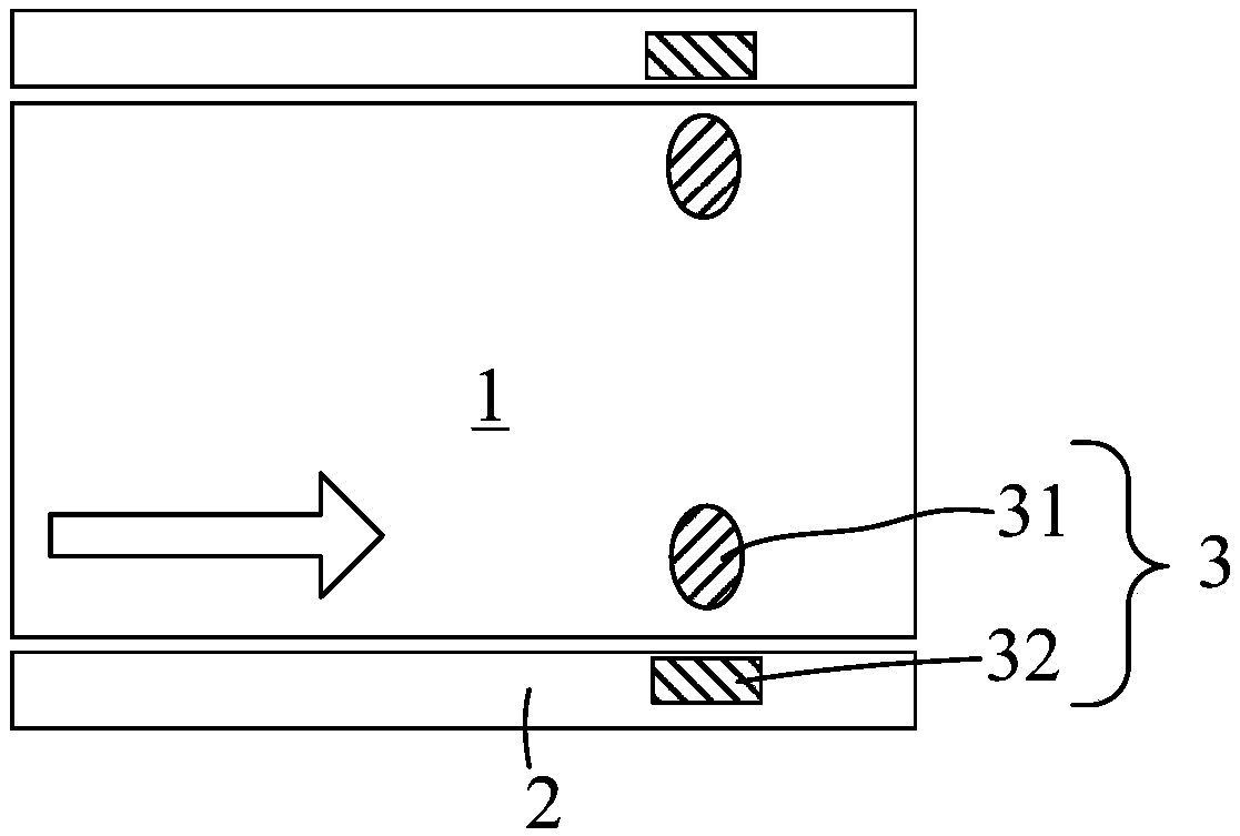
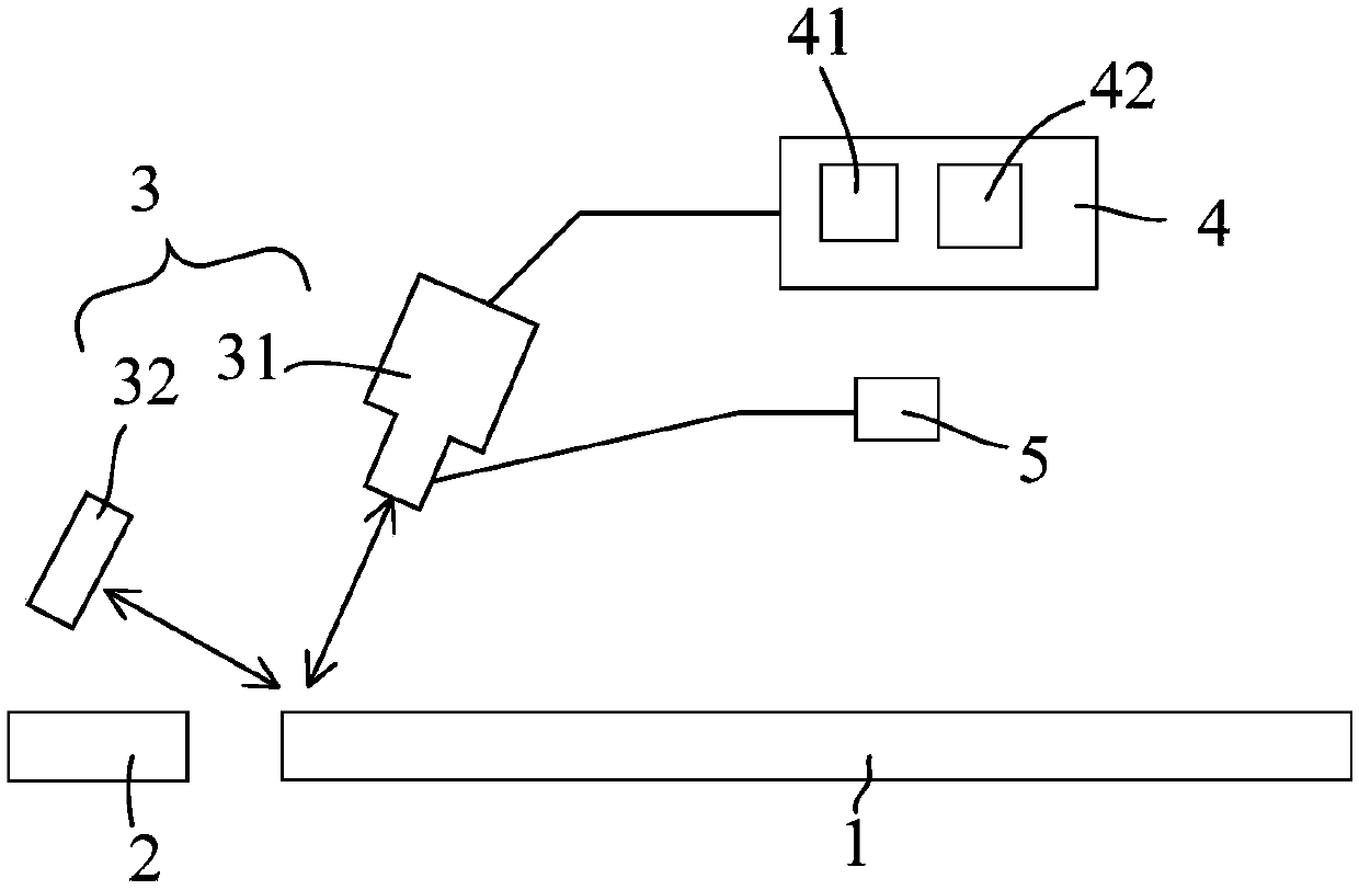
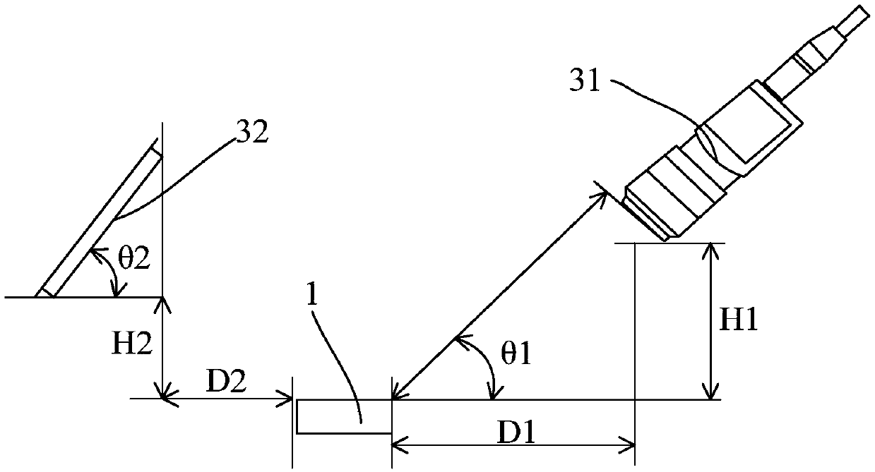
[0025] The following descriptions of the various embodiments refer to the accompanying drawings to illustrate specific embodiments in which the present invention can be practiced. The directional terms mentioned in the pres...


PUM

PropertyMeasurementUnit
Wavelengthaaaaaaaaaa

Abstract

The invention provides a substrate detection system and a substrate detection method. The substrate detection system comprises a mounting platform, a visual optical detection device and a program logical control device, wherein the mounting platform is used for carrying and conveying a substrate provided with a recognition code; the visual optical detection device is arranged on the mounting platform, and comprises a charge coupled member and a light source; the charge coupled member is used for taking a plurality of pictures of the edge of the substrate continuously and recording corresponding time; the program logical control device is electrically connected with the charge coupled member, and is used for judging the pictures; when the pictures are judged to have defects, a warning signal is generated, and a display screen of the program logical control device displays the recognition code and the time. Thus, the time and difficulty in finding substrate defects in the prior art is shortened and lowered effectively.

Description

technical field [0001] The invention relates to the field of substrate detection, in particular to a substrate detection system and a substrate detection method. Background technique [0002] In the thin film transistor device (TFT) manufacturing process, the glass substrate will have defects such as cracking / chipping due to the external force of conveying, loading / unloading by conveyor / robot, and process processing. In particular, when the glass substrate is broken during the stripping machine or the back-end process, it is impossible to trace and find the cause of the broken glass substrate. However, it is often difficult and time consuming to resolve the causes of chipping or cracking. Contents of the invention [0003] In view of this, it is necessary to provide a substrate detection system and a substrate detection method to solve the problems existing in the prior art. [0004] The purpose of the present invention is to provide a substrate detection system and a su...

Claims


Application Information

Patent Timeline
IPC IPC(8): G01N21/95
CPCG01N21/95G01N2021/9513
Inventor 陈建锋
Owner WUHAN CHINA STAR OPTOELECTRONICS SEMICON DISPLAY TECH CO LTD
Why Eureka
Try Eureka