

Packaging cover board, chip packaging structure and manufacturing method thereof
A technology of chip packaging structure and packaging cover plate, applied in semiconductor/solid-state device manufacturing, radiation control devices, electrical components, etc., can solve the problem of affecting the quality of optical components, low light penetration rate of chip packaging structure, and low light penetration rate and other issues, to achieve the effect of good light transmittance and improve process yield
- Summary
- Abstract
- Description
- Claims
- Application Information
AI Technical Summary
Problems solved by technology
Method used
Image

Examples
Embodiment Construction
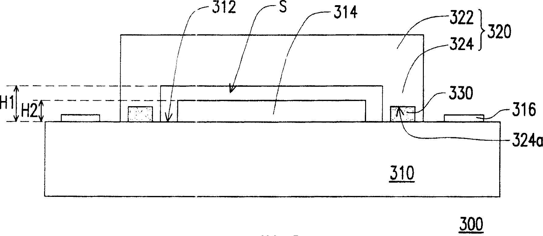
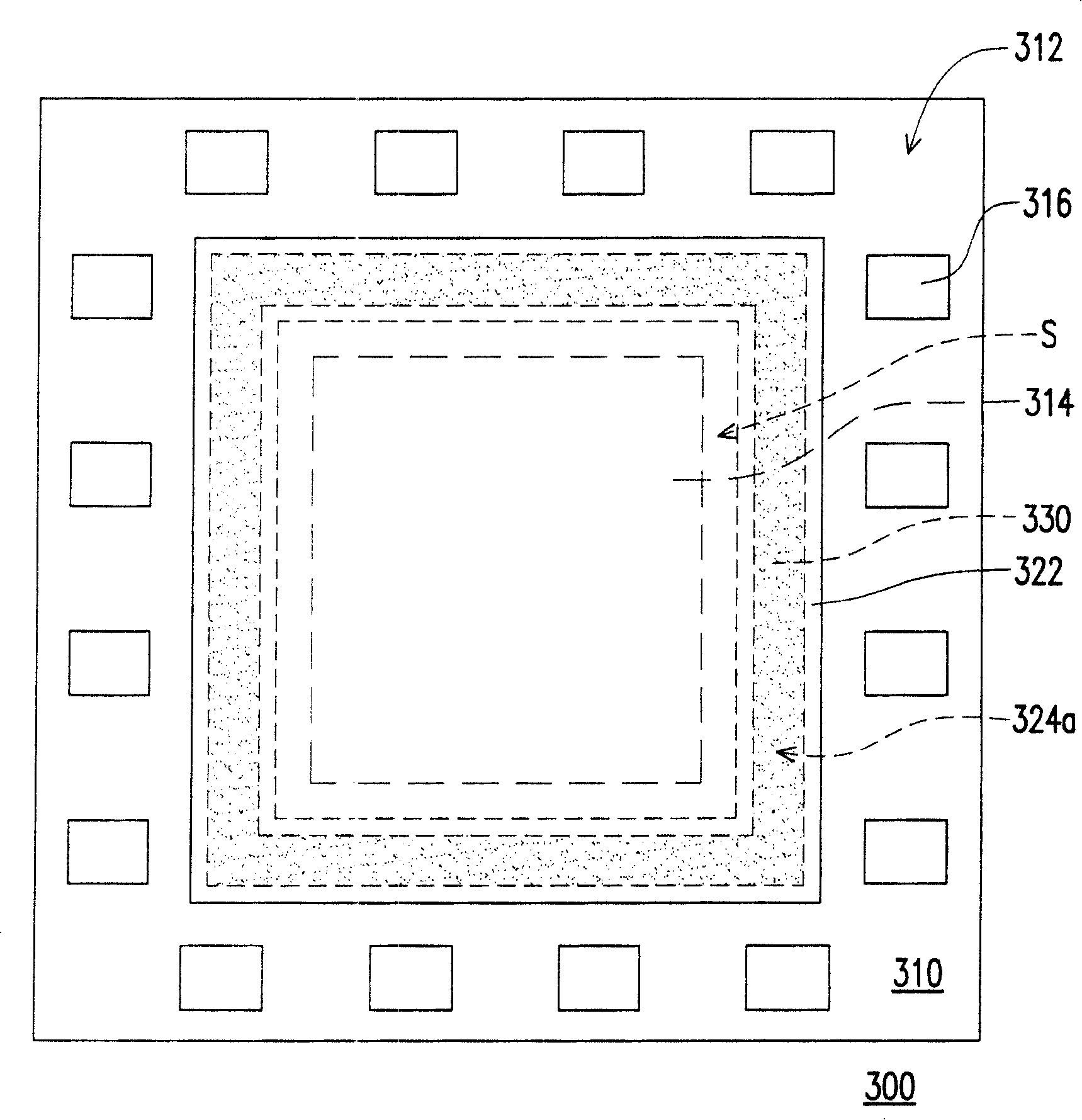
[0055] Please refer to figure 2 and image 3 , figure 2 A schematic cross-sectional view showing a chip packaging structure according to a preferred embodiment of the present invention, image 3 then draw figure 2 A schematic top view of the chip package structure. The chip package structure 300 of this embodiment includes a chip 310 , a package cover 320 and an adhesive layer 330 . Wherein, the chip 310 has an active surface 312 , and an image sensing element 314 and a plurality of pads 316 located around the image sensing element 314 are disposed on the active surface 312 . In one embodiment, the image sensing element 314 includes, for example, a contact image sensor or a complementary metal oxide semiconductor image sensor (CMOS image sensor), which is used to receive an external light signal, and transmit the light through the chip 310 The signal is converted into an electrical signal for processing. The image sensing element 314 is electrically connected to the s...
PUM
| Property | Measurement | Unit |
|---|---|---|
| Height | aaaaa | aaaaa |
Abstract
Description
Claims
Application Information