An electron beam focusing device with a high power density

A high power density, focusing device technology, applied in the direction of circuits, discharge tubes, electrical components, etc., can solve the problems of reduced electron beam current, low X-ray power density, and affecting X-ray focal spot size and power density. Achieve high power density, save material, and facilitate centering adjustment

Active Publication Date: 2019-04-05
INST OF ELECTRICAL ENG CHINESE ACAD OF SCI
View PDF8 Cites 2 Cited by
  • Summary
  • Abstract
  • Description
  • Claims
  • Application Information

AI Technical Summary

Problems solved by technology

If a multi-stage lens is simply used to reduce the small electron beam spot, its angular magnification will increase accordingly. In order to ensure the paraxial relationship in the actual lens system, the aperture of the diaphragm in the electron beam channel is generally small, and the electron beam cannot Effectively through the focusing system with large angular magnification, the electron beam current bombarding the target surface is reduced; therefore, it is difficult for the usual multi-lens focusing system to ensure that the electron beam bombarding the target surface has both large beam current and small beam current. beam spot, which in turn affects the focal spot size and power density of the generated X-rays
[0004] Most of the X-ray source focusing systems for electron beam targeting are modified or referred to the magnetic lens used in electron microscopes. When the electron beam spot on the target surface is small, the beam current is also small, and the X-ray power density generated is not high, so it is difficult to obtain high resolution. clear image

Method used


Image

  • An electron beam focusing device with a high power density
  • An electron beam focusing device with a high power density
  • An electron beam focusing device with a high power density

Examples


Embodiment Construction

[0028] The technical solutions of the present invention will be clearly and completely described below in conjunction with the accompanying drawings. Apparently, the described embodiments are some of the embodiments of the present invention, but not all of them. Based on the embodiments of the present invention, all other embodiments obtained by persons of ordinary skill in the art without making creative efforts fall within the protection scope of the present invention.

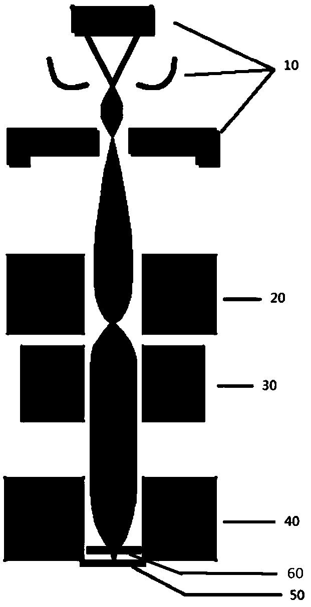
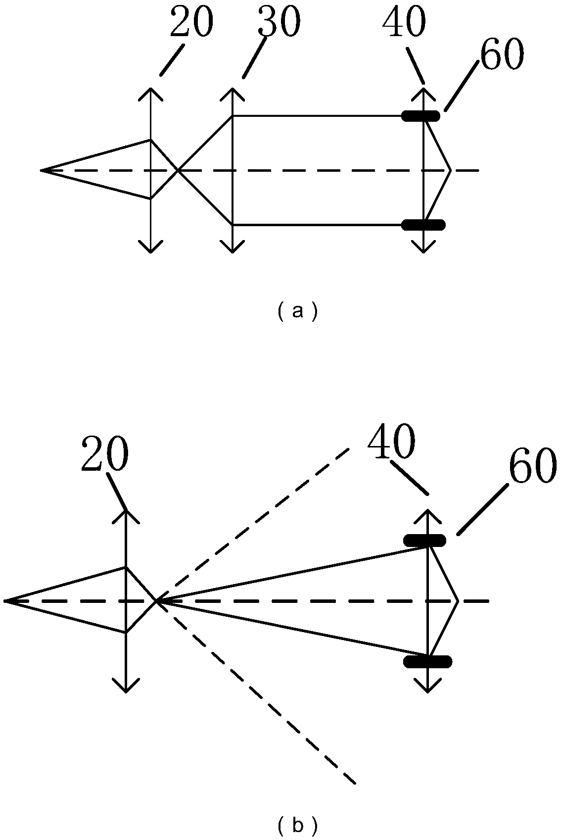
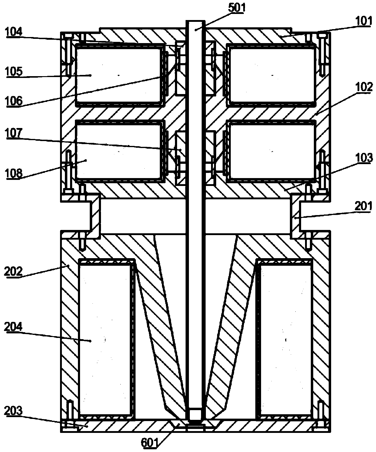
[0029] Such as figure 1 As shown, the embodiment of the present invention provides an electron beam focusing device, including: a condenser lens module 20, an auxiliary condenser lens module 30, an objective lens module 40, and an objective lens aperture module 60 arranged in sequence along the electron beam emission direction;

[0030] The condenser module 20 is used to form a first magnetic field, so that the electron beams form a cross point;

[0031] The auxiliary condenser module 30 is used to form a s...


PUM


Abstract

The invention discloses an electron beam focusing device with a high power density. The device comprises a collecting lens module, an auxiliary collecting lens module and an objective lens module arranged in sequence along an electron beam emitting direction; the collecting lens module is used to form a first magnetic field to enable an electron beam to form a cross point; the auxiliary collectinglens module is used to form a second magnetic field such that a movement trajectory of the electron beam is parallel to the optical axis to form a parallel beam, wherein the first magnetic field is greater than the second magnetic field in terms of the magnetic field strength; and the objective lens module is used to form a third magnetic field to focus the electron beam onto a target plane. A multi-lens combination mode of the collecting lens, the auxiliary collecting lens and the objective lens realizes the intersection, parallel and focus control of the electron beam, thereby obtaining thehigh reduction ratio and small aberration of the electron beam system and the high efficiency transmission of the beam current.

Description

technical field [0001] The invention belongs to the technical field of three-dimensional nondestructive microscopic observation, and in particular relates to an electron beam focusing device. Background technique [0002] High power density electron beam focusing devices can be used in imaging devices that use electron beams to bombard targets to generate corresponding rays to scan samples. For example, Micro-Computed Tomography (Micro-CT) is a technology that utilizes The non-destructive microscopic imaging technology, which scans the sample with X-rays and inverts the scanned data into a three-dimensional image, can display the internal structure, density and defects of the tested sample at the micron level or even sub-micron level, and has been widely used. It is the development direction of micro-CT technology to improve the detection resolution and efficiency when it is applied in the fields of life science, material science and geology. The X-ray source for electron b...

Claims


Application Information

Patent Timeline
Patent Type & Authority Applications(China)
IPC IPC(8): H01J37/10H01J37/256H01J37/26H01J37/30
CPCH01J37/10H01J37/256H01J37/261H01J37/3002
Inventor 刘俊标王丽娟赵伟霞王岩董增雅王鹏飞李文萍殷伯华韩立
Owner INST OF ELECTRICAL ENG CHINESE ACAD OF SCI
Why Eureka
Try Eureka