Trench type power semiconductor element and manufacturing method thereof

A technology for power semiconductors and manufacturing methods, which is applied in the fields of semiconductor/solid-state device manufacturing, semiconductor devices, electrical components, etc., can solve the problem of increasing electric field, reducing the withstand voltage of trench-type power metal-oxide-semiconductor field-effect transistors, and reducing the reliability of components, etc. question

Active Publication Date: 2019-04-05
SUPER GROUP SEMICON
View PDF3 Cites 2 Cited by
  • Summary
  • Abstract
  • Description
  • Claims
  • Application Information

AI Technical Summary

Problems solved by technology

The two sharp corners 101 and 102 at the bottom of the gate 10 will lead to an increase in the electric field and reduce the withstand voltage of the trench power metal oxide semiconductor field effect transistor, thereby reducing the reliability of the device

Method used


Image

  • Trench type power semiconductor element and manufacturing method thereof
  • Trench type power semiconductor element and manufacturing method thereof
  • Trench type power semiconductor element and manufacturing method thereof

Examples


Embodiment Construction

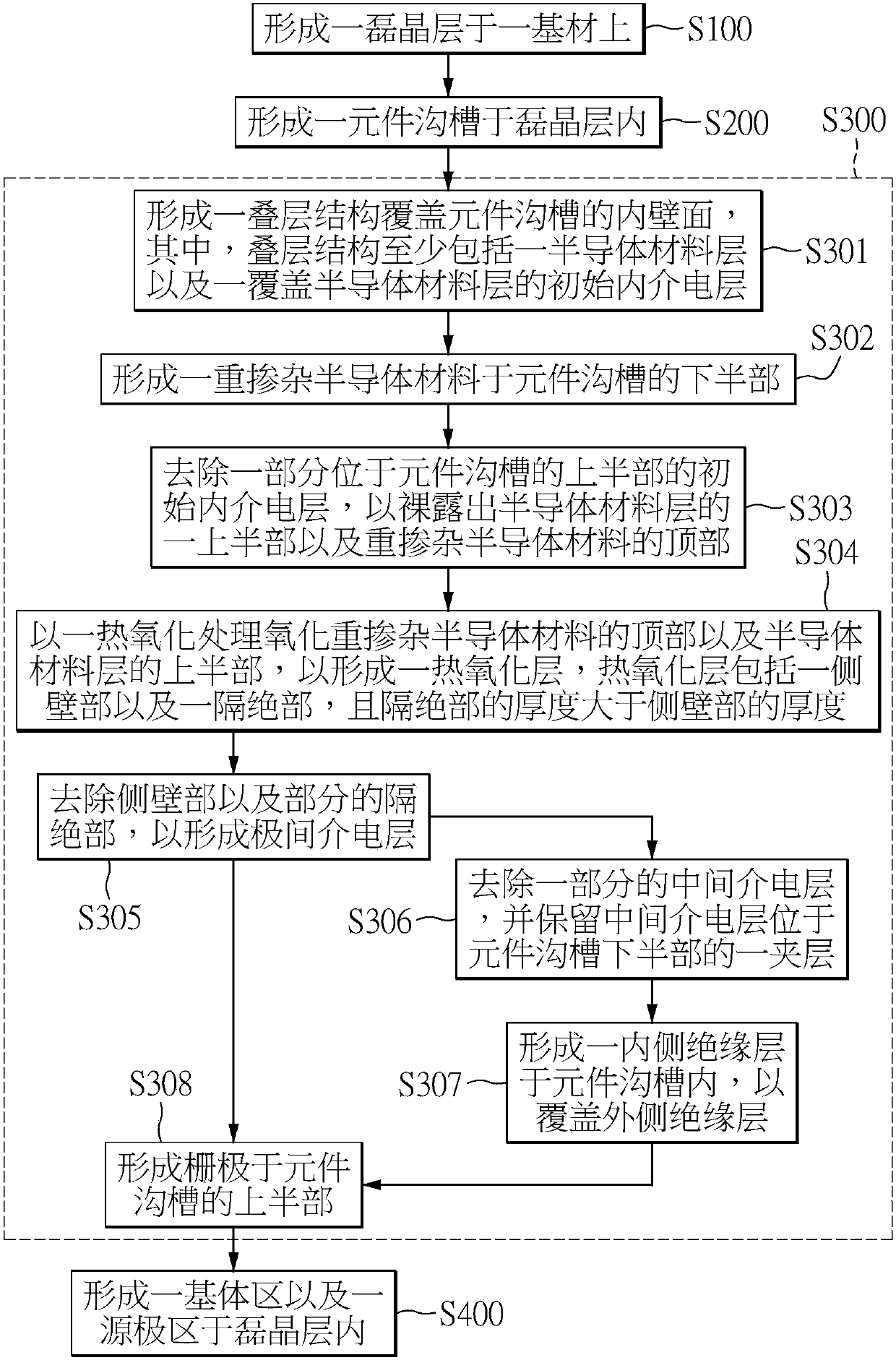
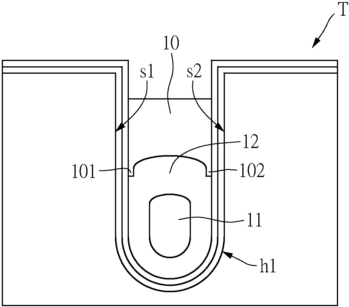
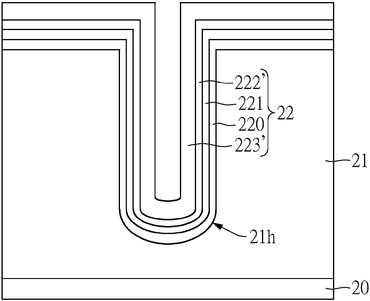
[0078] The following is an illustration of the implementation of the "trenched power semiconductor element and its manufacturing method" disclosed in the present invention through specific specific examples. Those skilled in the art can understand the advantages and effects of the present invention from the content disclosed in this specification. The present invention can be implemented or applied through other different specific embodiments, and various modifications and changes can be made to the details in this specification based on different viewpoints and applications without departing from the concept of the present invention. In addition, the drawings of the present invention are only for simple illustration, and are not drawn according to the actual size, which is stated in advance. The following embodiments will further describe the relevant technical content of the present invention in detail, but the disclosed content is not intended to limit the protection scope o...


PUM


Abstract

The invention discloses a trench type power semiconductor element and a manufacturing method thereof. The trench gate structure of the trench type power semiconductor element comprises a shielding electrode, a grid electrode located above the shielding electrode, and an inter-electrode dielectric layer located between the shielding electrode and the grid electrode. Before forming the inter-electrode dielectric layer, the step of forming the trench gate structure at least comprises the step that a laminated structure is formed to cover the inner wall surface of the element trench, wherein the laminated structure at least comprises a semiconductor material layer and an initial inner dielectric layer for covering the semiconductor material layer; a heavily-doped semiconductor material is formed at the lower half part of the element trench; and a part of the initial inner dielectric layer on the upper half part of the element trench is removed, so as to expose the upper half part of the semiconductor material layer and the top of the heavily-doped semiconductor material. Therefore, the bottom of the grid electrode formed in the subsequent manufacturing process can be prevented from having a sharp angle.

Description

technical field [0001] The invention relates to a power semiconductor element and a manufacturing method thereof, in particular to a trench type power semiconductor element with a shielding electrode and a manufacturing method thereof. Background technique [0002] The working loss of the existing trench power metal oxide semiconductor field effect transistor (Power Metal Oxide Semiconductor Field Transistor, Power MOSFET) can be divided into two categories: switching loss and conducting loss. The capacitance value of the drain (Cgd) is an important parameter affecting the switching loss. If the gate / drain capacitance value is too high, it will increase the switching loss, and then limit the switching speed of the power MOSFET, which is not conducive to the application in high frequency circuits. [0003] Accordingly, the existing trench power metal oxide half field effect transistor will have a shielding electrode (shielding electrode) located in the lower half of the gate...

Claims


Application Information

Patent Timeline
Patent Type & Authority Applications(China)
IPC IPC(8): H01L29/78H01L29/423H01L21/336H01L21/28
CPCH01L29/401H01L29/4236H01L29/66666H01L29/7827
Inventor 许修文
Owner SUPER GROUP SEMICON
Why Eureka
Try Eureka