Group III nitride semiconductor device and manufacturing method thereof

A technology of nitride semiconductors and nitrides, which is applied in the field of microelectronics, can solve the problems of current collapse, non-overlapping of forward curve and reverse curve, etc., to reduce the influence of current collapse effect, small gate leakage current, and reduce current The effect of the collapse effect

Active Publication Date: 2017-03-15
ENKRIS SEMICON
View PDF4 Cites 0 Cited by
  • Summary
  • Abstract
  • Description
  • Claims
  • Application Information

AI Technical Summary

Problems solved by technology

However, in the insulated gate field effect transistor manufactured by this method, there is a high density of interface states between the dielectric layer and the nitride semiconductor, which can cause serious current collapse effects, which is a big unresolved problem, such as figure 1 shown
Moreover, the insulating dielectric layer and the nitride semiconductor layer (such as Al 2 o 3 When there is a higher interface state between AlGaN and AlGaN), under forward bias, the charging and discharging of the interface state at the edge of the AlGaN conduction band will cause the hysteresis effect of the C-V curve of the device, that is, the forward curve and the reverse There will be a large degree of misalignment in the curves, such as figure 2 shown

Method used


Image

  • Group III nitride semiconductor device and manufacturing method thereof
  • Group III nitride semiconductor device and manufacturing method thereof
  • Group III nitride semiconductor device and manufacturing method thereof

Examples


Embodiment Construction

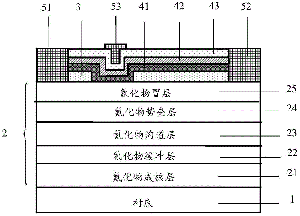
[0054] A group III nitride semiconductor device of the present invention, comprising:

[0055] Substrate;

[0056] A nitride semiconductor layer on the substrate, the nitride semiconductor layer includes a nitride nucleation layer, a nitride buffer layer, a nitride channel layer, and a nitride barrier layer formed sequentially from the direction of the substrate;

[0057] Preferably, a nitride capping layer may also be included between the nitride barrier layer and the passivation layer;

[0058] Preferably, the nitride capping layer includes a gallium nitride layer;

[0059] Preferably, an aluminum nitride insertion layer is provided between the nitride barrier layer and the nitride channel layer;

[0060] The passivation layer on the nitride semiconductor layer, the passivation layer is a combination of one or more of silicon nitride, silicon aluminum nitride, and silicon dioxide, and the passivation layer is etched in the gate region to expose nitrogen a compound barrier...


PUM

PropertyMeasurementUnit
thicknessaaaaaaaaaa
thicknessaaaaaaaaaa

Abstract

The invention discloses a Group III nitride semiconductor device and a manufacturing method thereof. The group III nitride semiconductor device includes a nitride semiconductor layer and a passivation layer grown on a substrate, and also includes a source and a drain and a gate between the source and the drain. Wherein, the above-mentioned nitride semiconductor layer includes a nitride nucleation layer, a nitride buffer layer, a nitride channel layer, and a nitride barrier layer; the above-mentioned passivation layer is etched in the gate region to expose the nitride barrier layer , forming grooves at the gate. In the present invention, a composite dielectric layer is used between the nitride barrier layer and the gate metal layer, including a combined structure of a nitride dielectric layer, an oxynitride dielectric layer and an oxide dielectric layer sequentially formed from the direction of the substrate. The composite dielectric layer structure does not cause an increase in the interface state density, and compared with the traditional III-nitride semiconductor device with a single-layer oxide dielectric layer, it can simultaneously reduce the leakage and current collapse effects of the semiconductor device.

Description

technical field [0001] The invention relates to the technical field of microelectronics, in particular to a Group III nitride semiconductor device and a manufacturing method thereof. Background technique [0002] Group III nitride semiconductors have the characteristics of wide band gap, high dielectric breakdown field strength and high electron saturation drift rate, which are suitable for manufacturing high-temperature, high-speed switching and high-power electronic devices. In a nitride field effect transistor, a large amount of charge is generated in the channel layer by piezoelectric polarization and spontaneous polarization. Since the source of the two-dimensional electron gas is the ionization of the donor surface state on the nitride surface, the current density of the nitride transistor is extremely sensitive to the surface state, and the existence of the surface state can easily cause the current collapse effect. [0003] Gallium nitride-based field effect transis...

Claims


Application Information

Patent Timeline
Patent Type & Authority Patents(China)
IPC IPC(8): H01L29/78H01L21/336
CPCH01L29/42364H01L29/513H01L29/518H01L29/66446H01L29/66522H01L29/78H01L29/4236H01L29/7786H01L29/2003H01L21/02178H01L21/0228H01L21/02326H01L29/511H01L29/66462H01L29/7787H01L21/0254H01L23/3171H01L29/517
Inventor 程凯
Owner ENKRIS SEMICON
Why Eureka
Try Eureka