Semiconductor device and method of manufacturing semiconductor device

A semiconductor and nitride semiconductor technology, applied in semiconductor/solid-state device manufacturing, semiconductor devices, electrical components, etc., to solve problems such as gate threshold voltage instability and operational failures

Active Publication Date: 2014-12-03
FUJITSU LTD
View PDF3 Cites 4 Cited by
  • Summary
  • Abstract
  • Description
  • Claims
  • Application Information

AI Technical Summary

Problems solved by technology

[0008] Incidentally, in a HEMT using a nitride semiconductor having a structure in which an insulating film is formed below...

Method used


Image

  • Semiconductor device and method of manufacturing semiconductor device
  • Semiconductor device and method of manufacturing semiconductor device
  • Semiconductor device and method of manufacturing semiconductor device

Examples


no. 1 example

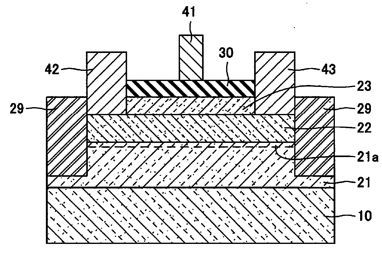
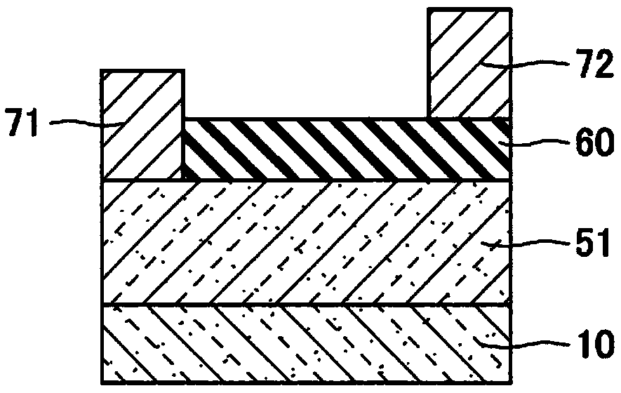
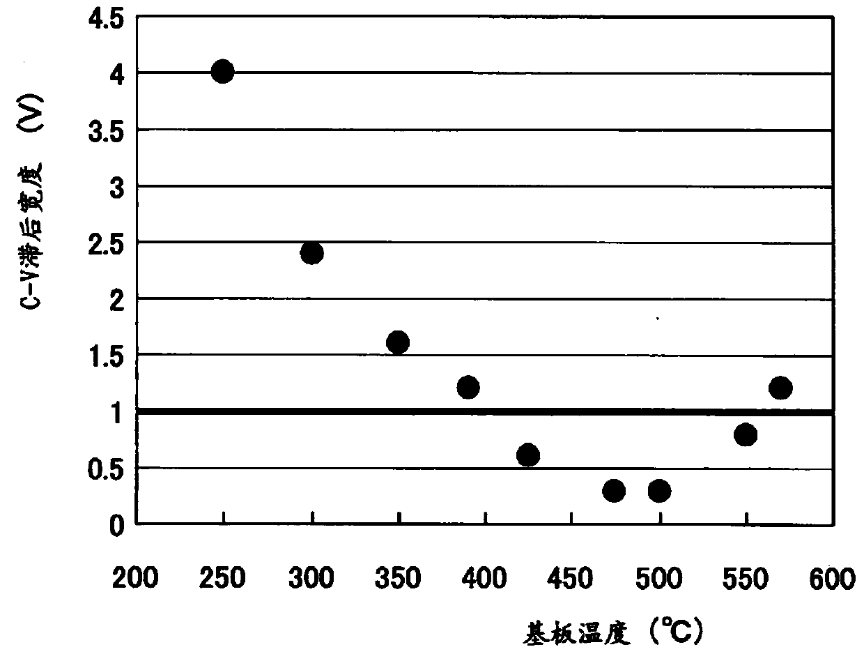
[0042] First, regarding HEMTs that use a nitride semiconductor having a structure in which an insulating film is formed below a gate electrode, there are figure 1 The semiconductor device of the structure shown has been fabricated by having figure 2 The C-V measurement sample of the structure shown was used to investigate the factors causing the gate threshold voltage to become unstable.

[0043] have figure 1 The semiconductor device of the structure has an electron transfer layer 21 , an electron supply layer 22 , and a protective layer 23 laminated on a substrate 10 and made of a nitride semiconductor. Furthermore, on a part of the electron transfer layer 21, the electron supply layer 22, and the protective layer 23, an element separation region 29 for separating elements is formed. On protective layer 23 , insulating layer 30 , source electrode 42 , and drain electrode 43 are formed, and on insulating layer 30 gate electrode 41 is formed. Note that, on the substrate 10...

no. 2 example

[0082] Next, based on Figure 14 A description is given of the second embodiment. The present embodiment has a structure in which insulating layers corresponding to portions where first insulating layer 131 and second insulating layer 132 are formed in the semiconductor device according to the first embodiment are formed by changing film formation conditions. Specifically, the semiconductor device according to this embodiment has a structure in which Al is formed on the protective layer 123 by ALD using TMA and oxygen plasma while gradually lowering the substrate temperature 2 o 3 , to form the insulating layer 230 . Therefore, the insulating layer 230 is formed such that the number of -OH groups is minimized near the interface between the insulating layer 230 and the protective layer 123, and the number of -OH groups gradually increases from the side where the protective layer 123 is formed toward the surface of the insulating layer 230. Increase. Note that the film thick...

no. 3 example

[0087] Semiconductor Device (Third Embodiment)

[0088] Next, based on Figure 15 A description is given of the semiconductor device according to the present embodiment. The semiconductor device according to the present embodiment has an electron transport layer 121 and an electron supply layer 122 which are laminated on a substrate 110 and made of a nitride semiconductor. Furthermore, on a part of the electron transfer layer 121 and the electron supply layer 122, an element separation region 129 for separating elements is formed. On the electron supply layer 122 , the stacked first insulating layer 131 and the second insulating layer 132 are formed together with the source electrode 142 and the drain electrode 143 . Furthermore, on the second insulating layer 132, a gate electrode 141 is formed. Note that, on the substrate 110, a buffer layer may be formed as necessary, and in this case, the above-described nitride semiconductor layer is formed on the buffer layer.

[008...


PUM

PropertyMeasurementUnit
Thicknessaaaaaaaaaa
Thicknessaaaaaaaaaa
Thicknessaaaaaaaaaa

Abstract

A semiconductor device includes a first semiconductor layer formed of a nitride semiconductor on a substrate; a second semiconductor layer formed of a nitride semiconductor on the first semiconductor layer; an insulating layer formed on the second semiconductor layer; a source electrode and a drain electrode formed on the second semiconductor layer; and a gate electrode formed on the insulating layer. The insulating layer is formed of a material including an oxide and is formed by laminating a first insulating layer and a second insulating layer in a positioning order of the first insulating layer followed by the second insulating layer from a side of the second semiconductor layer, and an amount of hydroxyl groups included in per unit volume of the first insulating layer is less than an amount of hydroxyl groups included in per unit volume of the second insulating layer.

Description

technical field [0001] Embodiments discussed herein relate to semiconductor devices and methods of manufacturing semiconductor devices. Background technique [0002] Materials made of GaN, AlN, and InN, which are nitride semiconductors, or mixed crystals thereof have a wide bandgap, and are used as high-output electronic devices or short-wavelength light-emitting devices. For example, GaN, which is a nitride semiconductor, has a band gap of 3.4 eV, which is wider than the band gap of 1.1 eV of Si and the band gap of 1.4 eV of GaAs. [0003] As such a high output device, there is a field effect transistor (FET), more specifically, a high electron mobility transistor (HEMT) (see, for example, Patent Document 1). HEMTs using such nitride semiconductors are used in high-output / high-efficiency amplifiers and high-power switching devices. Specifically, in HEMTs using AlGaN as the electron supply layer and GaN as the electron transfer layer, piezoelectric polarization occurs in A...

Claims


Application Information

Patent Timeline
IPC IPC(8): H01L29/778H01L29/06H01L29/08H01L21/335
CPCH01L29/66462H01L29/205H01L29/512H01L29/7783H01L29/2003H01L21/28264H01L29/41766H01L29/4236H01L29/513H01L29/517H01L29/7786
Inventor 金村雅仁
Owner FUJITSU LTD
Why Eureka
Try Eureka