Manufacture method of SiC DMISFET device of partitioned composite gate structure

A fabrication method and compound gate technology, applied in the field of microelectronics, can solve the problems of reducing interface state, high leakage current, high gate leakage current, etc.

Active Publication Date: 2015-07-29
DALIAN UNIV OF TECH +1
View PDF5 Cites 4 Cited by
  • Summary
  • Abstract
  • Description
  • Claims
  • Application Information

AI Technical Summary

Problems solved by technology

Although many research groups at home and abroad are working on improving SiC / SiO 2 A large number of experimental studies have been carried out on the interface quality, such as in NO or N 2 Gate oxidation or annealing in O atmosphere to remove SiC / SiO 2 The interface removes carbon residues, reduces interface traps, and improves the channel mobility of the inversion layer of the device. However, this method reduces the interface state and increases the fixed charge, causing a negative shift in the threshold voltage, causing the DMOS device to turn off. very high leakage current in the state
Based on this, high-K / SiO is currently used at home and abroad 2 stacked gate material to replace SiO 2 As the gate dielectric layer of SiCMIS devices, but studies have shown that there is still a high gate leakage current

Method used


Image

  • Manufacture method of SiC DMISFET device of partitioned composite gate structure
  • Manufacture method of SiC DMISFET device of partitioned composite gate structure
  • Manufacture method of SiC DMISFET device of partitioned composite gate structure

Examples


Embodiment 1

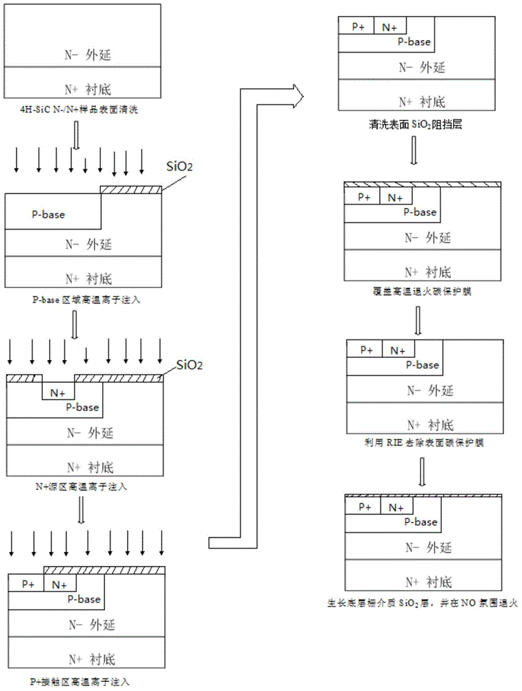
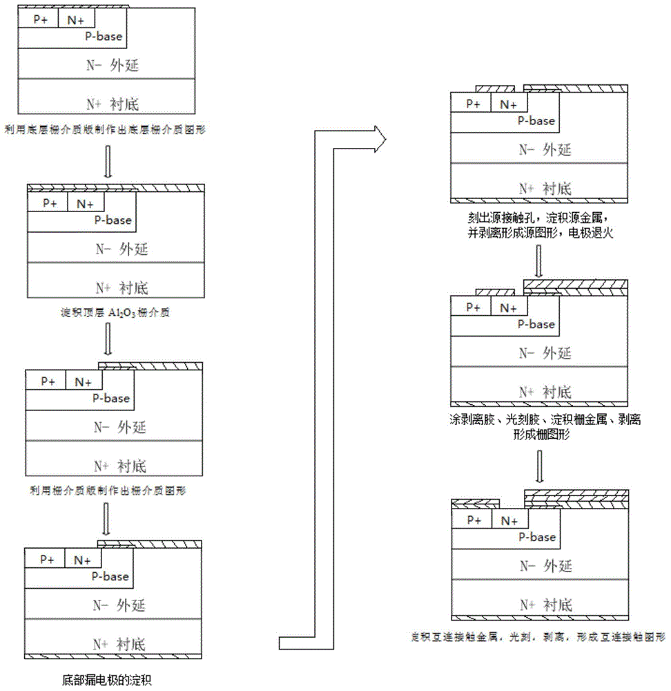
[0083] refer to figure 1 and 2 , the preparation and implementation steps of this embodiment are as follows:

[0084] Step 1, use the standard cleaning method RCA to clean the surface of the 4H-SiC N- / N+ type SiC epitaxial wafer:

[0085] (1a) Soak the 4H-SiC N- / N+ type SiC epitaxial wafer successively in acetone and absolute ethanol for 5 minutes each, and then rinse with deionized water to remove the grease on the surface of the SiC epitaxial wafer;

[0086] (1b) Place the SiC epitaxial wafer after the first cleaning in H 2 SO 4 :H 2 o 2 = 1:1 (volume ratio) soaked in the solution for 15min, H 2 SO 4 The concentration is 98%, H 2 o 2 The concentration is 27%, then rinse with deionized water;

[0087] (1c) Place the SiC epitaxial wafer after the second cleaning in HF:H 2 Soak in the solution of O=1:10 (volume ratio) for 1min to rinse off the natural oxide layer, the concentration of HF acid is 40%, and rinse with deionized water;

[0088] (1d) Dip the SiC epitaxia...

Embodiment 2

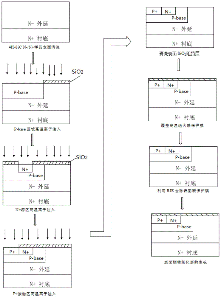
[0206] Compared with Example 1, in this example, on the basis of Example 1, the carbon protective film on the front of the N- / N+ SiC epitaxy is removed and Al is grown in a large area. 2 o 3 / Nitrided-SiO2 2 A growth process of a sacrificial oxide layer is added between the composite gate dielectric layers, which can more effectively reduce the interface damage caused by high-temperature ion implantation annealing, and effectively improve the flatness of the interface.

[0207] like image 3 and 4 As shown, the implementation steps of this embodiment 2 are as follows:

[0208] Step A, use the standard cleaning method RCA to clean the surface of the N- / N+ type SiC epitaxial wafer:

[0209] (Aa) Soak the N- / N+ type SiC epitaxial wafer in acetone and absolute ethanol for 5 minutes each, and then rinse with deionized water to remove the grease on the surface of the SiC epitaxial wafer;

[0210] (Ab) Place the SiC epitaxial wafer after the first cleaning in H 2 SO 4 :H 2 o ...


PUM

PropertyMeasurementUnit
thicknessaaaaaaaaaa

Abstract

The invention discloses a manufacture method of a SiC DMISFET device of a partitioned composite gate structure. The manufacture method comprises the steps that the surface of an N- / N+ type SiC epitaxial wafer is cleaned; a P-base area is etched, and Al ion implantation is carried out at high temperature; an N+ doped source area is etched, and N ion implantation is carried out at high temperature; a P type doped contact area is etched, and P type doped Al ion implantation is carried out at high temperature; a carbon protection film is formed at the surface of the N- / N+ type SiC epitaxial wafer; ion implantation annealing is carried out at the high temperature of 1600 DEG C; the carbon film at the surface is removed; acid cleaning is implemented; an Al2O3 / Nitrided-SiO2 composite gate dielectric layer is grown; a bottom drain electrode is grown; a peeling glue and a photoresist are coated, a source contact hole is etched, source metal is deposited, and a source pattern is peeled; gate electrode is formed on the SiC epitaxial wafer after annealing of the source and drain electrodes; and the source and drain interconnected electrode is formed, and a finished device is obtained. The manufacture method can effectively reduce the gate leakage current and improve the quality of the gate dielectric layer.

Description

technical field [0001] The invention relates to the technical field of microelectronics, in particular to a method for manufacturing a SiC DMISFET device with a partitioned composite gate structure. to reduce SiC / SiO 2 The interface state density reduces the electric field strength in the gate dielectric layer, reduces the FN tunneling current, improves the reliability of the gate dielectric layer, thereby improving its reliability in high temperature and high power applications. Background technique [0002] SiC has unique physical, chemical and electrical properties, and is a semiconductor material with great development potential in extreme applications such as high temperature, high frequency, high power and radiation resistance. The optimal working state of SiC power MOSFET is closely related to the interface characteristics and body characteristics of the gate dielectric insulating layer. The reliability of the gate dielectric layer has become the main problem that n...

Claims


Application Information

Patent Timeline
Patent Type & Authority Applications(China)
IPC IPC(8): H01L21/336H01L29/78H01L21/28
CPCH01L21/28255H01L29/401H01L29/42364H01L29/66068H01L29/7816
Inventor 刘莉杨银堂
Owner DALIAN UNIV OF TECH
Why Eureka
Try Eureka