JFET and manufacturing method thereof

A manufacturing method and deep well technology, applied in semiconductor/solid-state device manufacturing, electrical components, circuits, etc., can solve problems such as increased leakage current, unadjustable structure, JFET burning, etc., to suppress gate leakage current and reduce current Density, the effect of increasing the process window

Active Publication Date: 2018-07-20
SHANGHAI HUAHONG GRACE SEMICON MFG CORP
View PDF3 Cites 4 Cited by
  • Summary
  • Abstract
  • Description
  • Claims
  • Application Information

AI Technical Summary

Problems solved by technology

[0009] At the same time, in the existing JFET structure, as the drain terminal voltage rises, the leakage current at the gate terminal of the JFET will increase sharply, and eventually the JFET will be turned on and burned.
[0010] And because the JFET vertical channel is formed by the fixed process of the P-type well region 104 and the N-type deep well 102, that is, when the structure of the LDMOS is real, the process of the P-type well region 104 and the N-type deep well 102 It will be fixed, which makes the structure of the channel region of the JFET unadjustable, so it is difficult to achieve a higher pinch-off voltage, so that it cannot meet the customer's special design needs for the pinch-off voltage

Method used


Image

  • JFET and manufacturing method thereof
  • JFET and manufacturing method thereof
  • JFET and manufacturing method thereof

Examples


Embodiment J

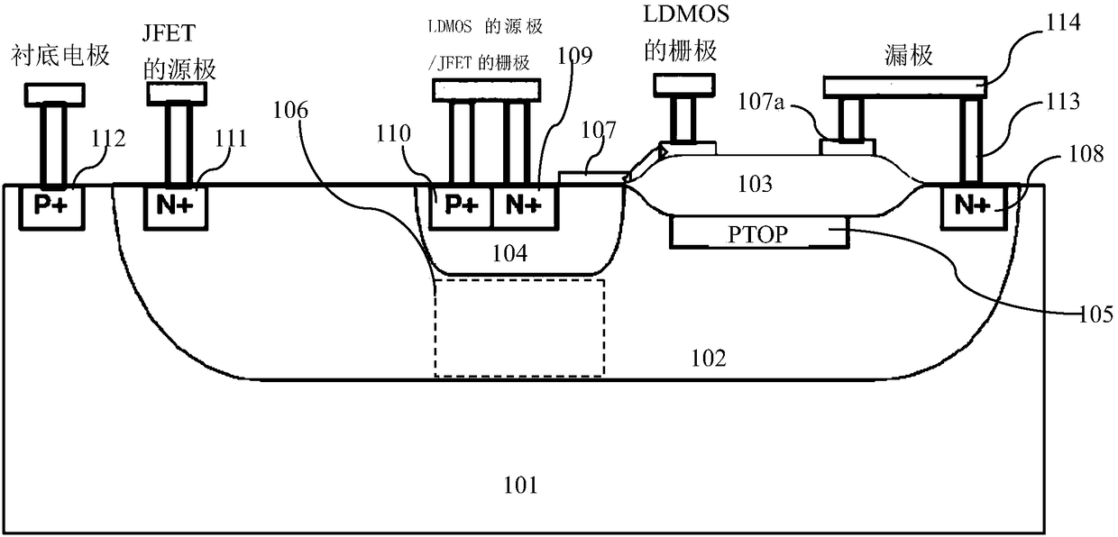
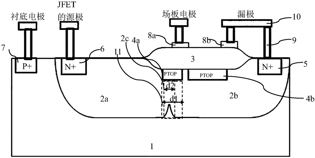
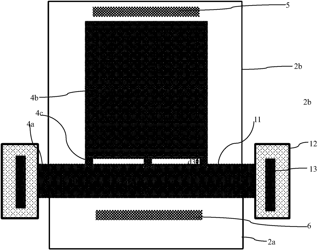
[0064] Such as Figure 2A Shown is the sectional view of JFET of the embodiment of the present invention; Figure 2B Shown is the layout of the JFET of the embodiment of the present invention; the JFET of the embodiment of the present invention includes:

[0065] An N-type deep well is formed on a P-type doped semiconductor substrate 1. The N-type deep well is formed by laterally splicing a first deep well segment 2a and a second deep well segment 2b. The first deep well segment 2a There is a gap with the implanted region of the second deep well segment 2b and is formed simultaneously by the same process, and the implanted gap regions of the first deep well segment 2a and the second deep well segment 2b form the channel resistance of the JFET Regulation area 2c.

[0066] A drift region field oxygen 3 is formed in the surface region of the N-type deep well, and a P-type top layer structure is formed on the surface of the N-type deep well at the bottom of the drift region fiel...


PUM


Abstract

The invention discloses a JFET. The JFET includes an N type deep well formed by transverse splicing of first and second deep well sections, and a channel resistance adjusting region of the JFET is formed between the two deep well sections; a P type top layer including a first top layer, a second top layer and a top layer connecting section is formed at the bottom of a drift region field oxygen thefirst top layer serves as a grid electrode region of the JFET, the N type deep well covered by the grid electrode region of the JFET serves as a channel region of the JFET, and the channel resistanceadjusting region is located in a channel region of the JFET; and the first top layer also extends into a semiconductor substrate on an outer side of the N type deep well and is connected to a grid electrode of the JFET through a contact hole. The invention also discloses a method for manufacturing a JFET. According to the JFET and manufacturing method thereof provided by the invention, pinch-offvoltage of a device can be increased, channel region resistance can be increased, and grid electrode leak current of the JFET can be reduced; and the JFET can be integrated with an LDMOS, and processcost is low.

Description

technical field [0001] The invention relates to the field of semiconductor integrated circuits, in particular to a junction field effect transistor (JFET); the invention also relates to a method for manufacturing the JFET. Background technique [0002] JFET uses the PN junction as the gate of the device to control the opening and closing of the channel. When the PN junction is negatively biased on the gate, both sides of the PN junction are depleted. When the channel is completely depleted, the device is in the pinch-off state of the channel. due. Otherwise, the device turns on. [0003] The ultra-high voltage junction field effect transistor needs the drain to withstand high voltage. Usually, the N-type deep well of the high-voltage LDMOS is used as the N-type deep well of the JFET to withstand high voltage, and the channel of the high-voltage LDMOS is used as the gate of the JFET, so that ultra-high voltage can be produced. JFET can also share the photolithography plate ...

Claims


Application Information

Patent Timeline
Patent Type & Authority Applications(China)
IPC IPC(8): H01L29/808H01L21/337
CPCH01L29/66893H01L29/66901H01L29/808
Inventor 王惠惠
Owner SHANGHAI HUAHONG GRACE SEMICON MFG CORP
Why Eureka
Try Eureka