Ferroelectric field effect transistor based on alumina material with embedded nanocrystalline and preparation method thereof

An electric field effect, alumina technology, applied in the field of large-scale integrated circuits and field effect transistors, can solve the problems of unstable device operation, cross-contamination between ferroelectric thin films and silicon integrated circuits, etc., to improve device performance, avoid cross-contamination, The effect of reducing gate leakage current

Active Publication Date: 2019-05-07
XIDIAN UNIV
View PDF4 Cites 5 Cited by
  • Summary
  • Abstract
  • Description
  • Claims
  • Application Information

AI Technical Summary

Problems solved by technology

[0009] The purpose of the present invention is to provide a ferroelectric field effect transistor based on aluminum oxide material with embedded nanocrystals and its preparation method, so as to avoid cross-contamination between the ferroelectric thin film and the silicon integrated circuit, and to overcome the problem of poor operation of the device when the thickness of the ferroelectric thin film is lower than 10nm. Stability, and the problem of crystallization required to form hafnium oxide-based ferroelectric thin films, improve the overall performance of the device

Method used


Image

  • Ferroelectric field effect transistor based on alumina material with embedded nanocrystalline and preparation method thereof
  • Ferroelectric field effect transistor based on alumina material with embedded nanocrystalline and preparation method thereof
  • Ferroelectric field effect transistor based on alumina material with embedded nanocrystalline and preparation method thereof

Examples


Embodiment 1

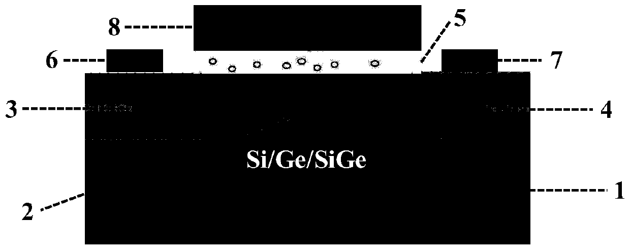
[0030] Embodiment 1: A p-type ferroelectric field effect transistor based on aluminum oxide material embedded with nanocrystals is prepared on a Ge substrate.

[0031] refer to figure 2 , the implementation steps of this example are as follows:

[0032] Step A: forming an aluminum oxide material embedded nanocrystalline ferroelectric thin film gate dielectric layer, such as figure 2 b.

[0033] A1) Standard cleaning of Ge substrates:

[0034] a1) Put the substrate into acetone, isopropanol and deionized water in sequence, and sonicate for 10 minutes each;

[0035] a2) Soak the substrate after ultrasonication in a mixed solution of hydrofluoric acid and water at a ratio of 1:50 for 1 min, and then rinse with deionized water for 2 min to complete the standard cleaning of the Ge substrate;

[0036] A2) Deposit aluminum oxide material with embedded nanocrystalline ferroelectric thin film gate dielectric layer:

[0037] Using atomic layer deposition technology, solid tetraki...

Embodiment 2

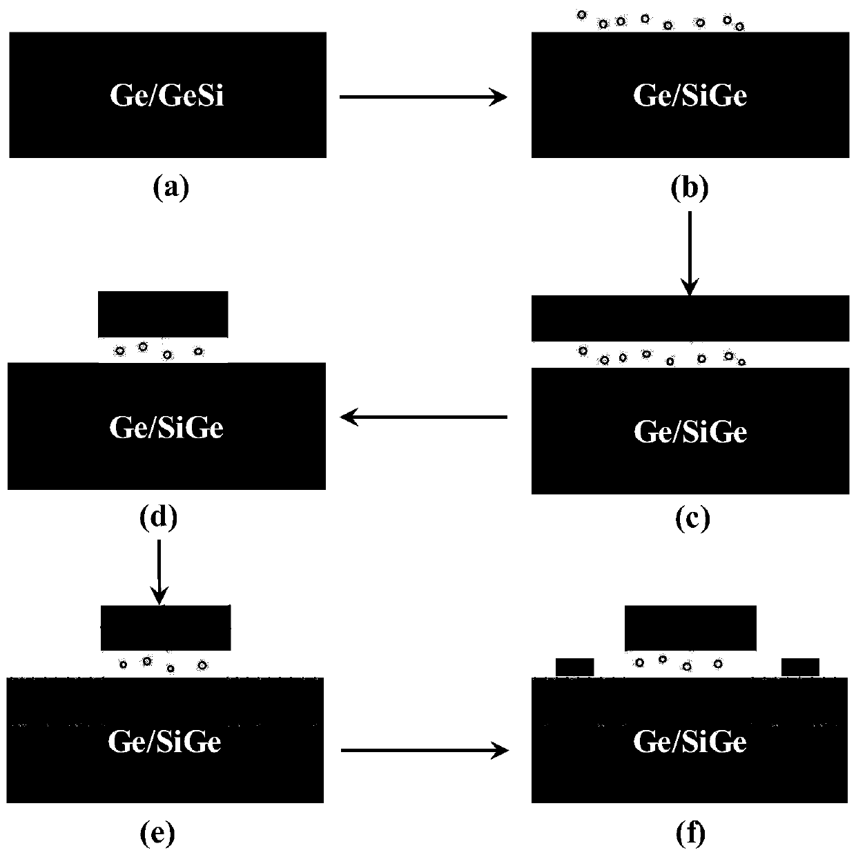
[0051] Example 2: On Si 0.55 Ge 0.45 A p-type ferroelectric field effect transistor embedded with nanocrystals in alumina material is prepared on a substrate.

[0052] refer to figure 2 , the specific implementation of this example is as follows:

[0053] Step 1: Forming an aluminum oxide material embedded nanocrystalline ferroelectric thin film gate dielectric layer, such as figure 2 b.

[0054] 1.1) Standard cleaning Si 0.55 Ge 0.45 Substrate:

[0055] 1.1.1) The specific realization of this step is the same as a1) in step A of embodiment 1;

[0056] 1.1.2) Soak the substrate after ultrasonication in a mixed solution of concentrated sulfuric acid and hydrogen peroxide at a ratio of 3:1 for 20 minutes;

[0057] 1.1.3) The specific realization of this step is the same as a2) in step A of embodiment 1;

[0058] 1.2) Deposit alumina material with embedded nanocrystalline ferroelectric thin film gate dielectric layer:

[0059] Using atomic layer deposition technology,...

Embodiment 3

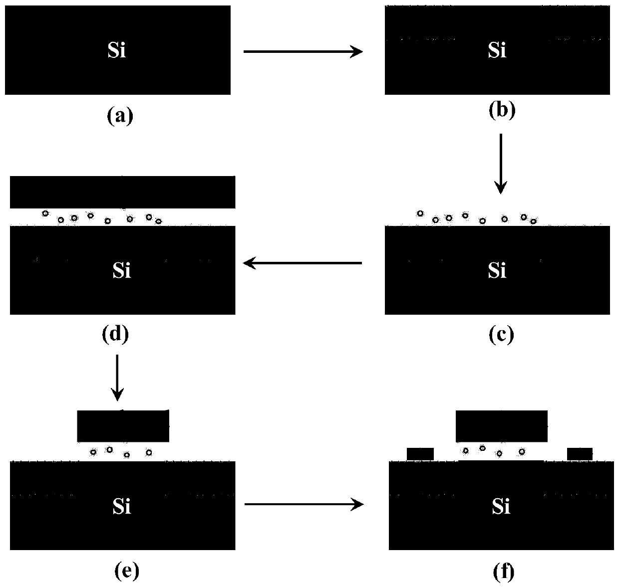
[0072] Embodiment 3: An n-type ferroelectric field effect transistor based on aluminum oxide material embedded with nanocrystals is prepared on a Si substrate.

[0073] refer to image 3 , the implementation steps of this embodiment are as follows:

[0074] Step 1: standard cleaning of the Si substrate, the specific implementation of this step is the same as that of step 1.1) of Embodiment 2.

[0075] The second step: mark the substrate area on the Si substrate.

[0076] Using 365nm I-line photolithography process, mark the source region, gate region, and drain region on the Si substrate, where the gate region is located in the center of the Si substrate, and the source region and drain region are respectively located at the center of the gate region. sides.

[0077] Step 3: Forming source and drain regions, such as image 3 b.

[0078] Under the masking effect of photoresist, ion implantation is performed on the source region and drain region after photolithography:

[...


PUM

PropertyMeasurementUnit
thicknessaaaaaaaaaa
lengthaaaaaaaaaa
thicknessaaaaaaaaaa

Abstract

The invention discloses a ferroelectric field effect transistor based on alumina material with embedded nanocrystalline and a preparation method thereof. The problems are mainly solved that a conventional ferroelectric gate dielectric in the current ferroelectric field effect transistor is incompatible with the prior art, and the hafnium oxide-based ferroelectric thin film generates large electricleakage. The ferroelectric field effect transistor comprises from bottom to top: a substrate (1), a channel (2), a gate dielectric layer (5) and a gate electrode (8); the two sides of the channel (2)are respectively provided with a source region (3) and a drain region (4); the upper portion of the source region (3) is provided with a source (6), and the upper portion of the drain region (4) is provided with a drain (7). The gate dielectric layer (5) employs an alumina ferroelectric film with an embedded nanocrystal. The ferroelectric field effect transistor based on alumina material with embedded nanocrystalline and the preparation method thereof can be compatible with the current integrated circuit process, can reduce the thickness of the gate dielectric layer below 4 nm, can reduce theelectric leakage of the gate dielectric layer, can improve the overall performances of the device and can be used for a large-scale integrated circuit.

Description

technical field [0001] The invention belongs to the technical field of microelectronic devices, in particular to a field-effect transistor embedded with a nanocrystalline ferroelectric gate medium, which can be used for large-scale integrated circuits. Background technique [0002] The electronic information industry plays an extremely important role in expanding social employment, promoting economic growth, enhancing international competitiveness and maintaining national security. The new materials, new structures and new processes required for its development have always been listed as key development targets by semiconductor powers . Ferroelectric field effect transistors have the advantages of fast read and write response, low power consumption and non-destructive reading, and are indispensable in modern logic devices and memory devices. [0003] Ferroelectric field effect transistors add a layer of ferroelectric film to the gate dielectric layer. Common ferroelectric m...

Claims


Application Information

Patent Timeline
Patent Type & Authority Applications(China)
IPC IPC(8): H01L29/78H01L21/336H01L29/423B82Y30/00B82Y40/00
Inventor 韩根全彭悦朱明璋张春福张进成郝跃
Owner XIDIAN UNIV
Why Eureka
Try Eureka