Automatic PCB cleaning and detecting device

A PCB board, automatic cleaning technology, applied in cleaning methods and utensils, cleaning methods using tools, conveyors, etc., can solve problems such as fatigue, affecting work efficiency, PCB board cleaning quality, and affecting the accuracy of PCB inspection results. , to achieve the effect of improving accuracy, improving cleaning efficiency and cleaning quality, and saving labor costs

Inactive Publication Date: 2019-04-09
哈工大机器人义乌人工智能研究院
View PDF7 Cites 2 Cited by
  • Summary
  • Abstract
  • Description
  • Claims
  • Application Information

AI Technical Summary

Problems solved by technology

Before the electronic components are welded on the PCB board, it needs to be inspected by a PCB detector (currently commonly used PCB inspection instruments include NV small-stroke automatic optical imager, NV large-stroke automatic optical imager and SFV static fast detector), However, the PCB board needs to be cleaned before the PCB board inspection. The current PCB board cleaning is usually done by manual cleaning, that is, the operator holds the cleaning brush to clean the surface of the PCB board, and the manual cleaning operation is performed for a long time. It is not only prone to fatigue, but also affects work efficiency and PCB board cleaning quality, and poor PCB board cleaning quality will affect the accuracy of PCB inspection results

Method used


Image

  • Automatic PCB cleaning and detecting device
  • Automatic PCB cleaning and detecting device
  • Automatic PCB cleaning and detecting device

Examples


specific Embodiment 1

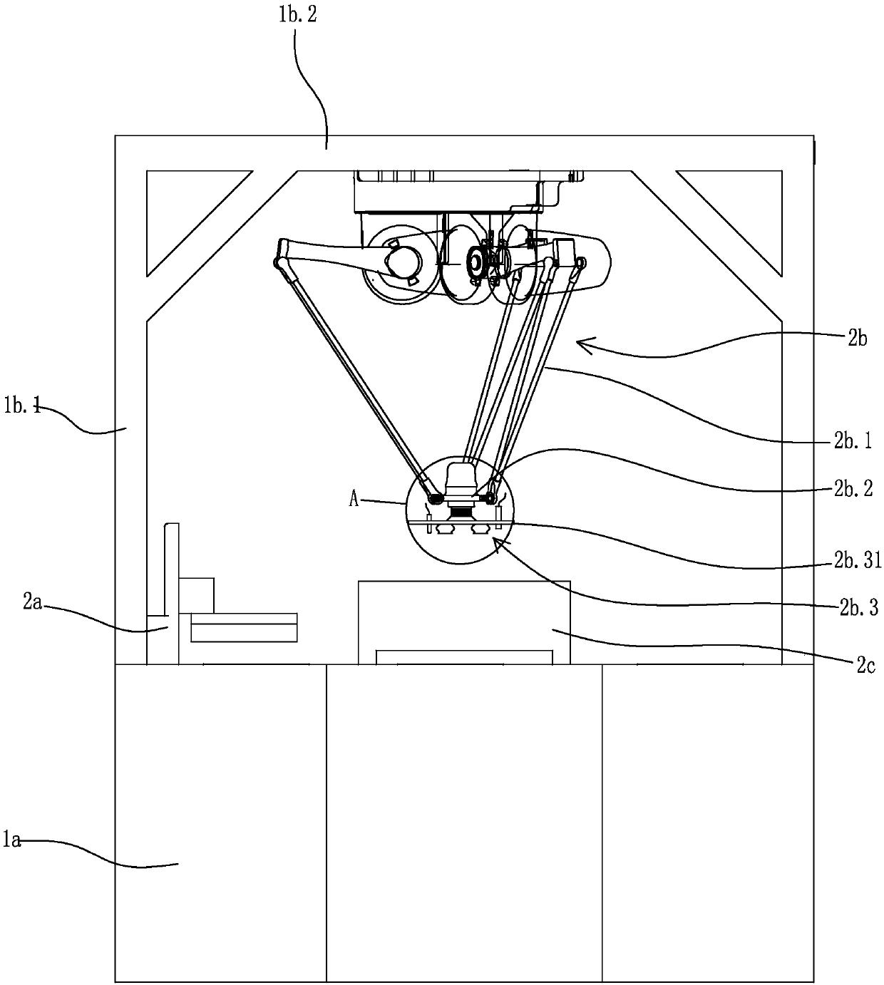
[0050] Specific embodiment one: as figure 1 , figure 2 As shown, a PCB board automatic cleaning and testing equipment includes a machine table, a spider hand robot 2b, a PCB board cleaning device 2a and a PCB testing instrument 2c.

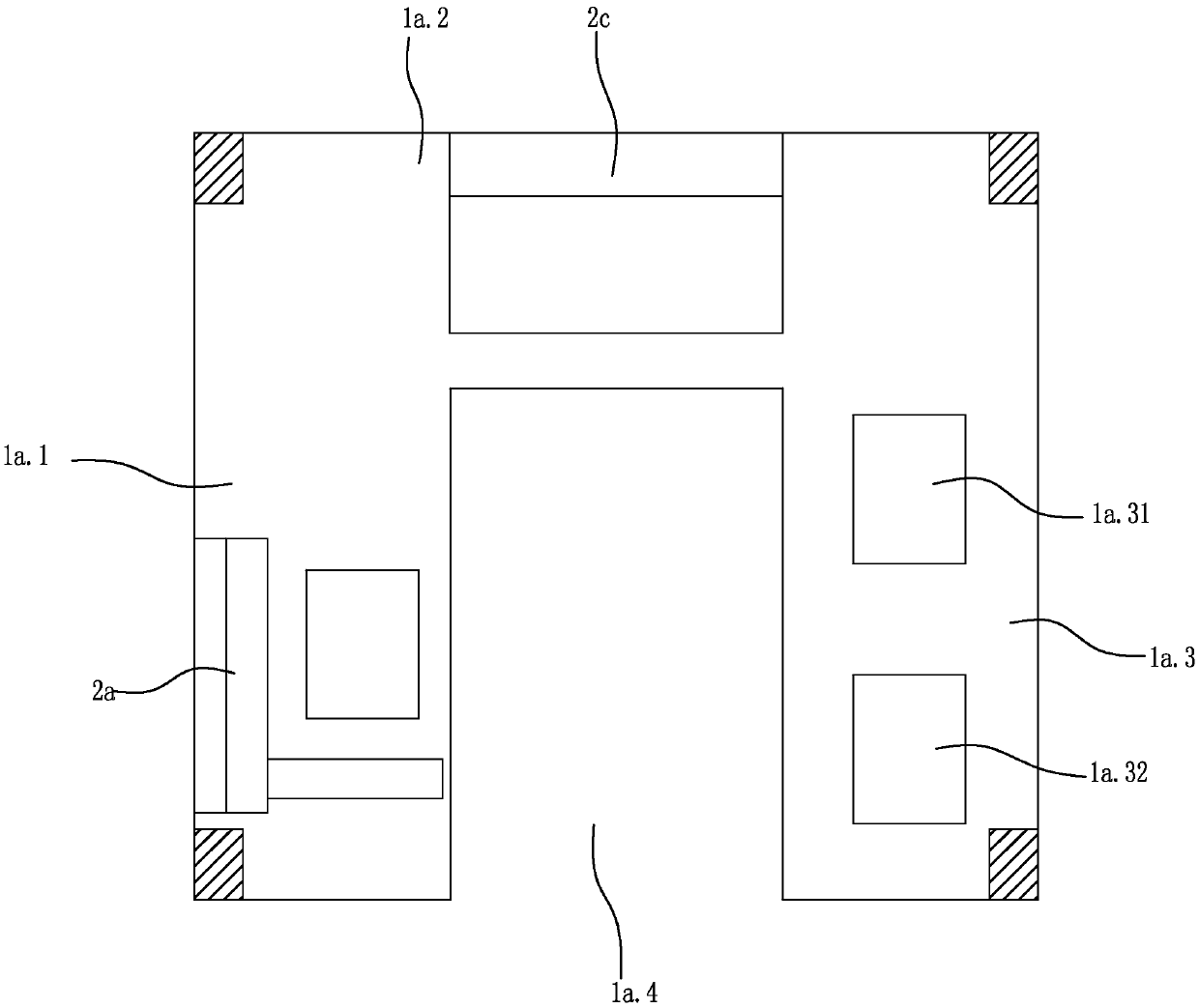
[0051] The machine platform includes a general worktable 1a and a frame arranged on the general workbench. The frame includes a side support 1b.1 and a top support 1b.2 arranged on top of the side support.

[0052] The general workbench includes a cleaning workbench 1a.1, a detection workbench 1a.2 and an output workbench 1a.3. The cleaning workbench, the detection workbench and the output workbench are connected in sequence. The cleaning workbench, detection workbench and output workbench are distributed in a U shape. The space between the cleaning workbench, the detection workbench and the output workbench forms the operation space 1a.4. The output workbench is provided with qualified product output station 1a.31 and unqualified product o...

specific Embodiment 2

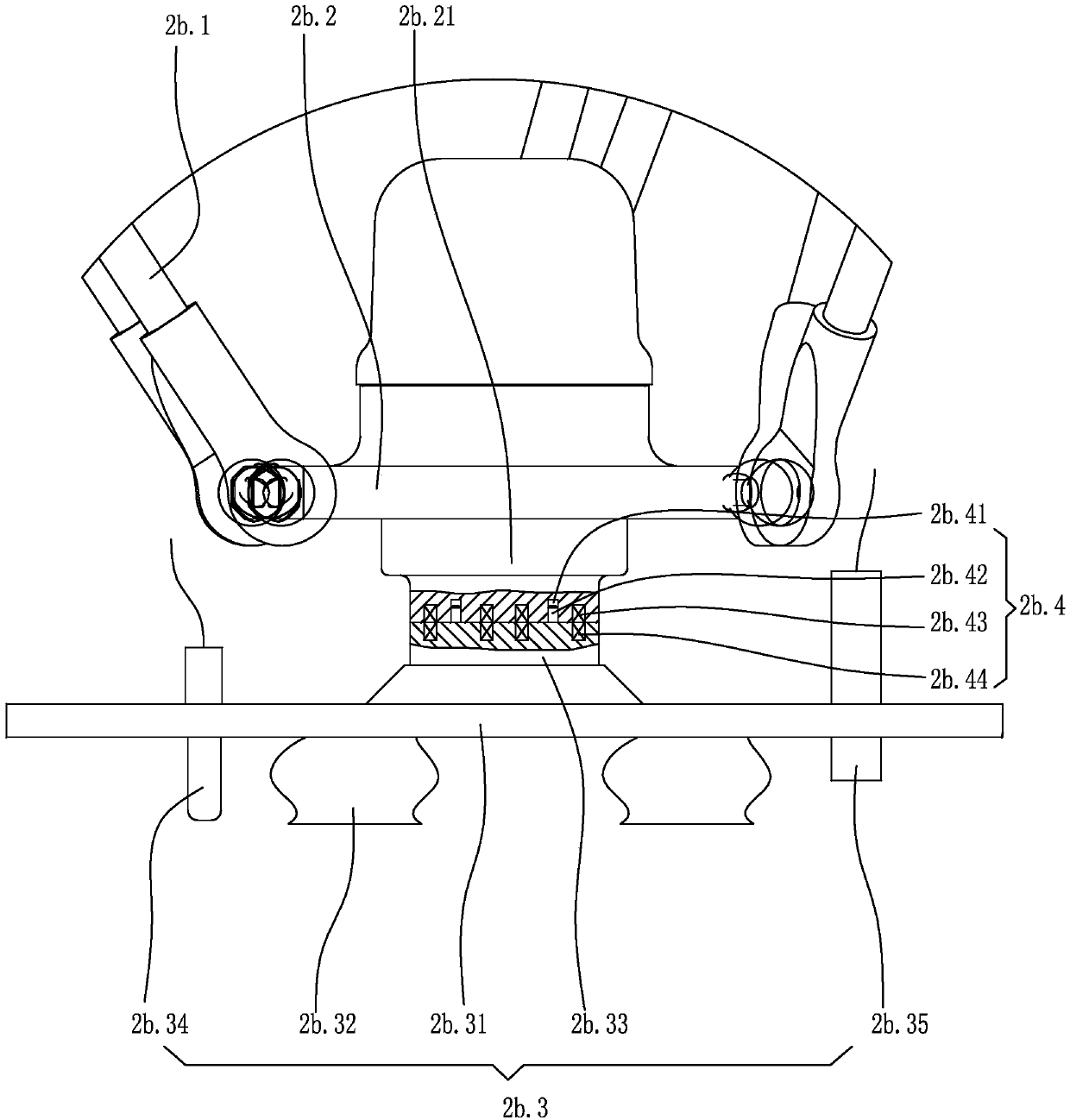
[0084] Specific embodiment two: the specific structure of this embodiment is with reference to specific embodiment one, and its difference is: as figure 2 As shown, the PCB board adsorption device includes a contact sensor 2b.34 provided on the conveying board. The controller is electrically connected with the contact sensor. When the spider hand robot controls the mounting plate and the PCB adsorption device to move down and absorb the PCB board, when the contact sensor touches the PCB board to be adsorbed, the controller controls the spider hand robot to stop the mounting plate from moving down, and at this time , The suction cup of the PCB board adsorption device absorbs the PCB board; in this way, the excessive downward movement of the PCB board adsorption device can be avoided, causing the PCB board to be crushed.

specific Embodiment 3

[0085] Specific embodiment three: the specific structure of this embodiment refers to specific embodiment one or specific embodiment two, and its difference is: as figure 2 As shown, the PCB board adsorption device includes a laser distance measuring sensor 2b.35 set on the conveying board. The controller is electrically connected with the laser ranging sensor. When the spider hand robot controls the mounting plate and the PCB adsorption device to move down and absorb the PCB board, the laser ranging sensor can detect the distance between the carrier board and the PCB board to be adsorbed. When the carrier board is close to the PCB board to be adsorbed At this time, the controller controls the spider hand robot to reduce the downward movement speed of the mounting plate and the PCB board adsorption device, so as to avoid excessive downward movement of the PCB board adsorption device and cause the PCB board to be crushed.


PUM


Abstract

The invention discloses an automatic PCB cleaning and detecting device. By adoption of the automatic PCB cleaning and detecting device, the surfaces of PCBs can be automatically cleaned, so that the labor cost is reduced, the PCB cleaning efficiency and quality are improved, and accordingly, the accuracy of PCB detection results is improved. The automatic PCB cleaning and detecting device comprises a machine table, a PCB cleaning device and a PCB detector. The machine table comprises a main workbench and a machine frame arranged on the main workbench. The main workbench comprises a cleaning workbench, a detecting workbench and an output workbench which are connected in sequence. The machine frame comprises a top frame and a spider claw robot mounted on the top frame. The spider claw robotcomprises a mounting disc mounted at the lower end of a rotary shaft of the spider claw robot and a PCB suction device arranged on the mounting disc. The PCB suction device comprises a transferring plate and a plurality of suction cups arranged on the lower surface of the transferring plate. The PCB cleaning device is arranged on the cleaning workbench. The PCB detector is arranged on the detecting workbench.

Description

technical field [0001] The invention relates to a PCB board detection device, in particular to a PCB board automatic cleaning and detection device. Background technique [0002] PCB board is called printed circuit board, also known as printed circuit board and printed circuit board. It is an important electronic component, a support for electronic components, and a provider of electrical connections for electronic components. Because it is made using electronic printing, it is called a "printed" circuit board. Before the electronic components are welded on the PCB board, it needs to be tested by a PCB detector (currently commonly used PCB testing instruments include NV small-stroke automatic optical imager, NV large-stroke automatic optical imager and SFV static fast detector), However, the PCB board needs to be cleaned before the PCB board inspection. The current PCB board cleaning is usually done by manual cleaning, that is, the operator holds a cleaning brush to clean th...

Claims


Application Information

Patent Timeline
IPC IPC(8): B65G47/91B08B1/00
CPCB65G47/917B65G2203/044B65G2201/022B65G2207/08B08B1/12
Inventor 何俊屠一峰孙博马明媚费天祥
Owner 哈工大机器人义乌人工智能研究院
Why Eureka
Try Eureka