Chip surface-mounting identification system and method

A chip placement and identification system technology, applied in the field of optical communication, can solve the problems of placement accuracy, influence placement accuracy, system complexity, etc., to shorten the slow stroke and eliminate the impact of position deviation on placement accuracy. , Improve the effect of patch efficiency

Active Publication Date: 2019-04-12
WUHAN TELECOMM DEVICES
View PDF6 Cites 4 Cited by
  • Summary
  • Abstract
  • Description
  • Claims
  • Application Information

AI Technical Summary

Problems solved by technology

However, by setting up two cameras for position recognition, the system is more complicated, and the relative position between the two cameras will also cause a certain recognition error. When the relative position of the two cameras fluctuates, the mounting accuracy will be affected; On the other hand, the identification of the chip position may change to a certain extent after the chip is picked up by the suction head before the chip is picked up, that is, there may be a certain position deviation before and after the chip is picked up, and the chip moves with the suction head. During the process, the position deviation of the chip relative to the suction head cannot be eliminated, and it will also affect the placement accuracy. Moreover, since the stroke from the chip position recognition to the chip transfer to the substrate for placement is relatively long, in order to reduce air resistance. Influenced by chip absorption stability, the movement speed of the welding head during the entire stroke should not be too fast, which will affect the placement efficiency

Method used


Image

  • Chip surface-mounting identification system and method
  • Chip surface-mounting identification system and method
  • Chip surface-mounting identification system and method

Examples


Embodiment 1

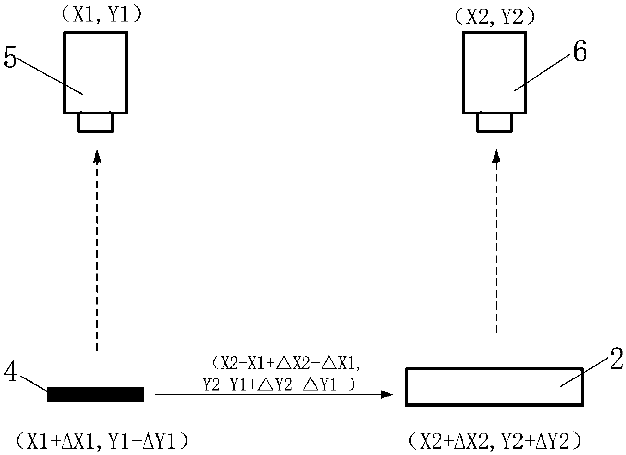
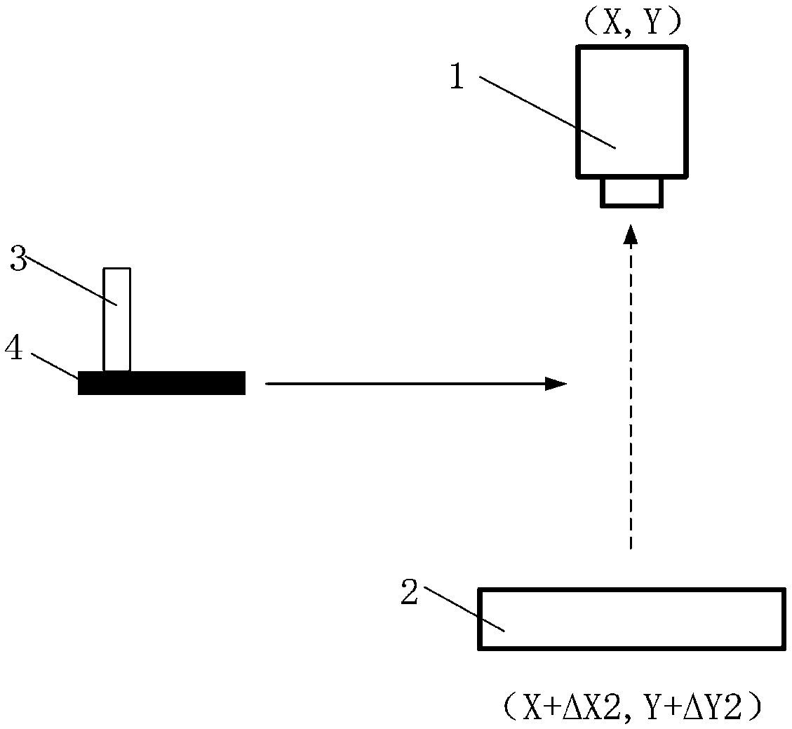
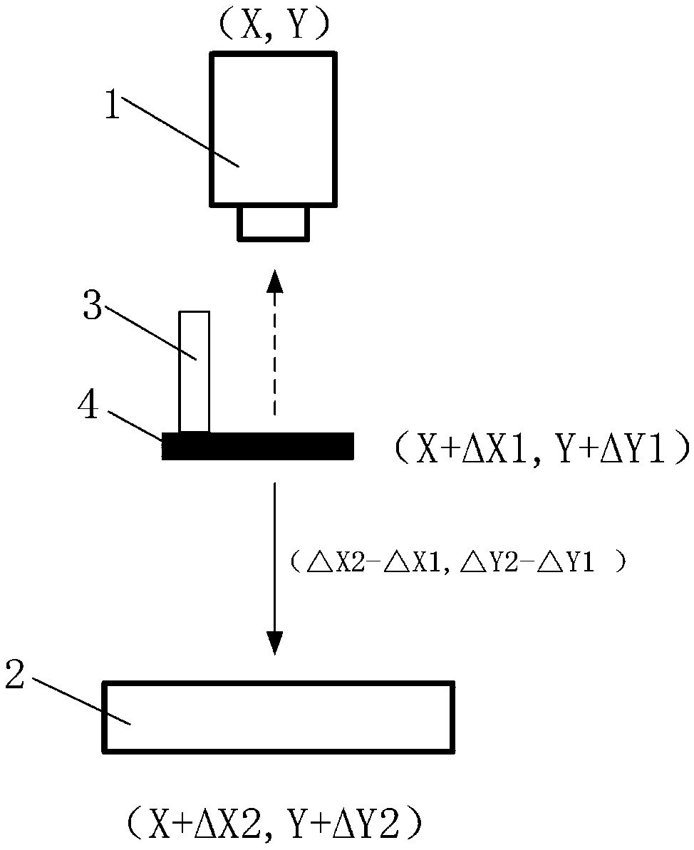
[0044] An embodiment of the present invention provides a chip mounting recognition system, such as figure 2 and image 3 As shown, it includes a photographing device 1, a substrate 2 and an adsorption device 3, the photographing device 1 is located above the substrate 2, the substrate 2 is used for mounting the chip 4, and the adsorption device 3 is used for adsorbing the chip 4 and The chip 4 moves below the photographing device 1, specifically between the photographing device 1 and the substrate 2, the photographing device 1 is used to photograph the substrate 2 and the chip 4, and then identify them by photographing The position of the substrate 2 and the position of the chip 4;

[0045] Wherein, an identification area is provided on the surface of the chip 4, and the identification area can be exposed when the adsorption device 3 absorbs the chip 4, so that when the chip 4 is moved to the bottom of the imaging device 1, the imaging device 1 The identification area on th...

Embodiment 2

[0055] On the basis of the above-mentioned embodiment 1, the embodiment of the present invention also provides a chip mounting identification method, which can be completed by using the chip mounting identification system described in embodiment 1, such as Figure 7 As shown, the method specifically includes the following steps:

[0056] In step 201, the position recognition of the substrate is carried out by the photographing device above the substrate. Wherein, the photographing device 1 acquires the absolute coordinates of the substrate 2 by photographing the recognition point on the surface of the substrate 2; refer to figure 2 , the absolute coordinates of the photographing device 1 are marked as (X, Y), and the acquired absolute coordinates of the substrate 2 are (X+ΔX2, Y+ΔY2).

[0057] Step 202, pick up the chip and move it between the camera and the substrate, and identify the position of the chip by the camera. Such as figure 2 , the chip 4 is sucked by the suct...


PUM


Abstract

The invention relates to the technical field of optical communication, and provides a chip surface-mounting identifying system and method. The system comprises a shooting device, a substrate and an absorption device, wherein the shooting device is arranged on the substrate, the substrate is used for surface-mounting a chip, the absorption device is used for absorbing the chip and moving the chip to a part below the shooting device, the shooting device is used for identifying a position of the substrate and a position of the chip by shooting, an identification region is arranged on a surface ofthe chip, and the identification region is exposed when the absorption device absorbs the chip so that the chip is moved to the part below the shooting device, and the shooting device is used for identifying the position of the chip by shooting the identification region. By the system, the identification region of the surface can be exposed when the chip is absorbed by using the special absorption device; identification and positioning of the chip and the substrate are completed by a camera, the system cost is low, the influence of an installation error of different cameras on surface-mounting accuracy is eliminated, moreover, the chip position is identified after the chip is absorbed, and the surface-mounting accuracy and the surface-mounting efficiency are improved.

Description

【Technical field】 [0001] The invention relates to the technical field of optical communication, and provides a chip mounting identification system and method. 【Background technique】 [0002] The optical module is a kind of communication module that can complete the mutual conversion function of photoelectric signals. With the advent of the era of big data, the demand for optical modules for data communication is becoming more and more strong. The optical module is mainly composed of two parts: the circuit part and the optical path part. The circuit part is mainly used for the processing and transmission of electrical signals, and the optical path part is mainly responsible for the transmission of optical signals. During the production process of the optical module, the optical components related to the optical path are aligned. The process is more important, called optical path coupling or optical component coupling. With the improvement of integration density, more and mor...

Claims


Application Information

Patent Timeline
IPC IPC(8): H01L21/67H01L21/68H01L21/683H01L21/02
CPCH01L21/02H01L21/67294H01L21/681H01L21/6838
Inventor 周艳阳何明阳黄笛高繁荣付永安孙丽萍
Owner WUHAN TELECOMM DEVICES
Why Eureka
Try Eureka