
Charge voltage conversion amplification circuit and electronic device

A charge-voltage conversion and amplifying circuit technology, which is applied to charge amplifiers, components of amplifying devices, and negative feedback circuit layout, etc., can solve problems such as submersion of charge signals, and achieve the effect of improving performance indicators and increasing the success rate of processing.

Pending Publication Date: 2019-04-12
BAOJI UNIV OF ARTS & SCI
View PDF0 Cites 1 Cited by
  • Summary
  • Abstract
  • Description
  • Claims
  • Application Information

AI Technical Summary

Problems solved by technology

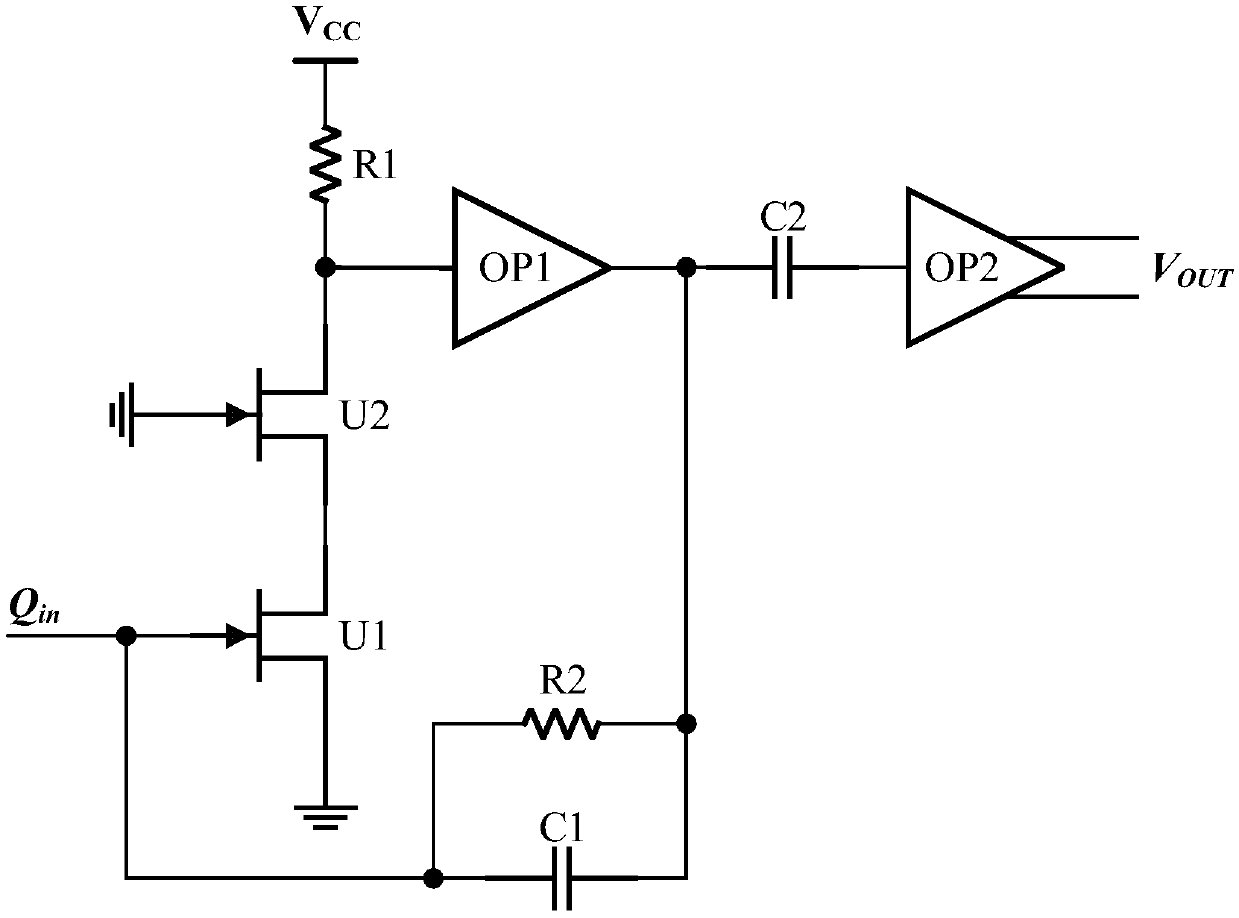
[0003] The purpose of this application is to solve the problem that the detected charge signal in the conventional charge processing circuit is easily completely submerged by noise, thus providing a charge-to-voltage conversion amplifier circuit and electronic device, wherein the charge-to-voltage conversion amplifier circuit detects The charge signal is amplified by a two-stage amplifier circuit. At the same time, the generation of noise is minimized in terms of circuit design and device selection, so that the charge signal is completely submerged by noise and the success rate of charge signal processing is improved.

Method used


Image

  • Charge voltage conversion amplification circuit and electronic device
  • Charge voltage conversion amplification circuit and electronic device
  • Charge voltage conversion amplification circuit and electronic device

Examples


Embodiment 1

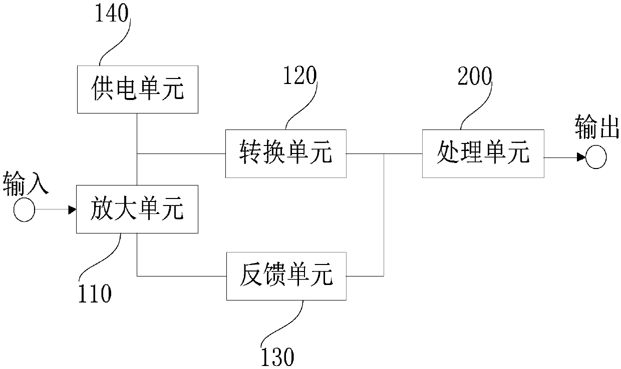
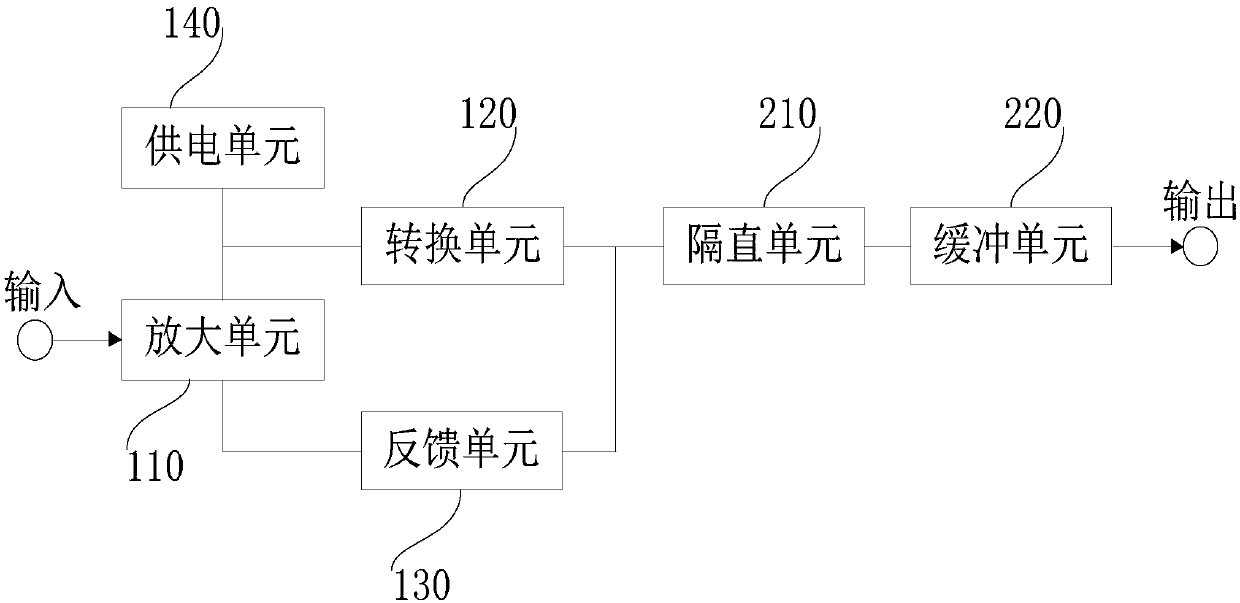
[0028] see figure 1 , the charge-to-voltage conversion amplifier circuit includes an amplification unit 110 , a conversion unit 120 , a feedback unit 130 and an output unit 200 .

[0029] The input terminal of the amplification unit 110 is used to connect the detector and amplify the charge signal output by the detector; the input terminal of the conversion unit 120 is connected to the output terminal of the amplification unit 110, and is used to convert the charge signal amplified by the amplification unit 110 into a preset Standard voltage signal; the input end of the feedback unit 130 is connected to the output end of the conversion unit 120 , and the output end is connected to the input end of the amplification unit 110 . The amplifying unit, the converting unit and the feedback unit form a closed loop, and the output terminal signal is fed back to the input terminal, which can improve the performance index of the amplifying circuit. The input end of the output unit 200 i...

Embodiment 2

[0039] Such as figure 1 As shown, the charge-to-voltage conversion amplifier circuit includes an amplification unit 110 , a conversion unit 120 , a feedback unit 130 and an output unit 200 .

[0040] The input terminal of the amplification unit 110 is used to connect the detector and amplify the charge signal output by the detector; the input terminal of the conversion unit 120 is connected to the output terminal of the amplification unit 110, and is used to convert the charge signal amplified by the amplification unit 110 into a preset Standard voltage signal; the input end of the feedback unit 130 is connected to the output end of the conversion unit 120 , and the output end is connected to the input end of the amplification unit 110 . The amplifying unit, the converting unit and the feedback unit form a closed loop, and the output terminal signal is fed back to the input terminal, which can improve the performance index of the amplifying circuit. The input end of the outpu...

Embodiment 3

[0050] see figure 1 As shown, the charge-to-voltage conversion amplifier circuit includes an amplification unit 110 , a conversion unit 120 , a feedback unit 130 and an output unit 200 .

[0051] The input terminal of the amplification unit 110 is used to connect the detector and amplify the charge signal output by the detector; the input terminal of the conversion unit 120 is connected to the output terminal of the amplification unit 110, and is used to convert the charge signal amplified by the amplification unit 110 into a preset Standard voltage signal; the input end of the feedback unit 130 is connected to the output end of the conversion unit 120 , and the output end is connected to the input end of the amplification unit 110 . The amplifying unit, the converting unit and the feedback unit form a closed loop, and the output terminal signal is fed back to the input terminal, which can improve the performance index of the amplifying circuit. The input end of the output un...


PUM


Abstract

The invention belongs to the technical field of circuits, and discloses a charge voltage conversion amplification circuit and an electronic device. The charge voltage conversion amplification circuitis used for amplifying a charge signal output by a charge detector and converting the amplified charge signal into a voltage signal of a preset specification. The charge voltage conversion amplification circuit comprises an amplification unit, a conversion unit, a feedback unit and an output unit, wherein the amplification unit is used for being connected with the detector and amplifying the charge signal output by the detector; the conversion unit is used for converting the charge signal amplified by the amplification unit into the voltage signal of the preset specification; the input end ofthe feedback unit is connected to the output end of the conversion unit, and the output end of the feedback unit is connected to the input end of the amplification unit; and the input end of the output unit is connected to the output end of the amplifier, and the output unit is used for processing the voltage signal after conversion by the conversion unit and outputting the voltage signal. The charge voltage conversion amplification circuit can reduce the generation of noises and improve the processing success rate of the charge signal.

Description

technical field [0001] The present application belongs to the technical field of circuits, relates to the technical field of charge signal processing, and in particular relates to a charge-voltage conversion amplifier circuit and an electronic device. Background technique [0002] In particle physics experiments, fast and accurate measurement of weak charge signals is a key factor affecting experimental results. Usually in a high-precision particle physics experiment system, the charge signal output by the detector is very weak, some even in the order of flying library, but the event rate is very high, and the conventional charge processing circuit cannot quickly process such a high event rate. A small signal causes the signal to be easily overwhelmed by noise, which greatly affects the accuracy of the entire experimental system and thus affects the experimental conclusion. Contents of the invention [0003] The purpose of this application is to solve the problem that the...

Claims


Application Information

Patent Timeline
Patent Type & Authority Applications(China)
IPC IPC(8): H03F1/34H03F1/26H03F3/70H03F3/68
CPCH03F1/26H03F1/342H03F3/68H03F3/70H03F2200/372
Inventor 张光南
Owner BAOJI UNIV OF ARTS & SCI
Learn More