An automatic feeding and testing device for pcb boards

A detection device and PCB board technology, applied in transportation and packaging, electronic circuit testing, mechanical conveyors, etc., can solve problems affecting product quality, affecting production automation process, low efficiency of integrated circuit board material and detection, etc., to reduce The effects of manual operation, improvement of detection speed and efficiency, and improvement of feeding efficiency

Active Publication Date: 2020-11-10
ANHUI DASHENG ELECTRONICS
View PDF10 Cites 0 Cited by
  • Summary
  • Abstract
  • Description
  • Claims
  • Application Information

AI Technical Summary

Problems solved by technology

[0003] The technical problem to be solved by the present invention is: the existing integrated circuit board feeding and detection efficiency is low, which affects product quality and also seriously affects the automation process of production

Method used


Image

  • An automatic feeding and testing device for pcb boards
  • An automatic feeding and testing device for pcb boards
  • An automatic feeding and testing device for pcb boards

Examples


Embodiment Construction

[0036] In order to facilitate those skilled in the art to understand the technical solution of the present invention, the technical solution of the present invention will be further described in conjunction with the accompanying drawings.

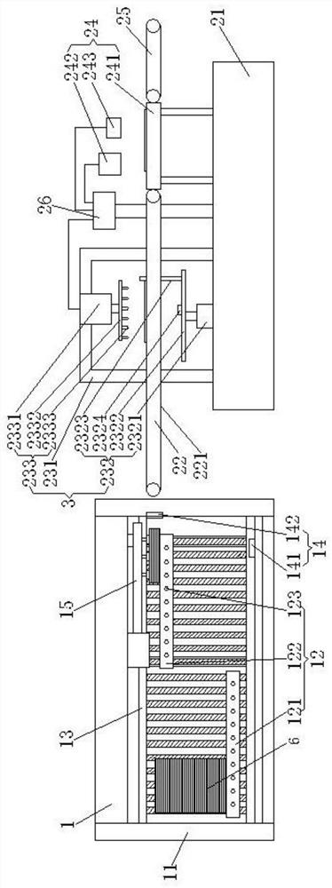
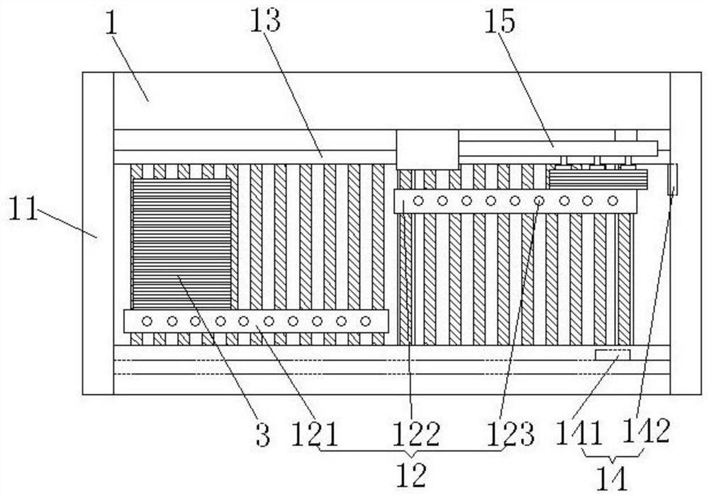
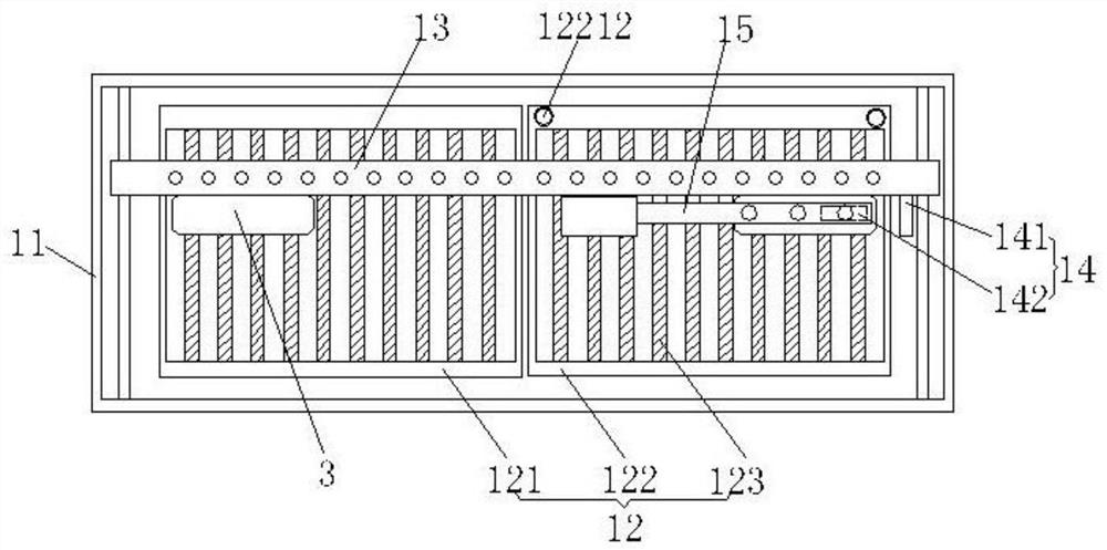
[0037] refer to Figure 1 to Figure 7 , this embodiment discloses an automatic loading and testing device for PCB boards, including a loading device 1 and a testing device 2, the loading device 1 is arranged before the testing device 2, and provides feeding services for the testing device 2.

[0038] The feeding device 1 includes a box body 11, a conveying platform 12, a movable limit device 13, an infrared sensing system 14, a mechanical sucker device 15 and an electrical control system (not shown in the figure), and the box body 11 is a cuboid hollow Box body, the box body 11 is provided with a conveying platform 12 , a movable limit device 13 and a mechanical sucker device 15 .

[0039] Described conveying platform 12 comprises fixed pl...


PUM


Abstract

The invention discloses an automatic feeding and detecting device for PCBs. The automatic feeding and detecting device comprises a feeding device and a detecting device. The feeding device is arrangedbefore the detecting device. The feeding device comprises a box body, a conveying platform, a movable limiting device, an infrared induction system, a mechanical sucker device and an electrical control system. The detecting device comprises a detecting platform, first conveying devices, an electricity detecting device, an optical detecting device, a second conveying device and a computer. The electricity detecting device is arranged between the first conveying devices. The computer, the optical detecting device and the second conveying device are sequentially arranged behind the electricity detecting device. The electricity detecting device and the optical detecting device are connected with the computer. The automatic feeding and detecting device has the advantages that the PCBs are fedin a centralized manner, the product quality is improved, the automatic production efficiency is improved, meanwhile, by means of the detecting device, electricity and optical detecting can be carriedout in the automatic conveying process of the PCBs, the detecting speed is increased, the detecting efficiency is improved, and manual operation is reduced.

Description

technical field [0001] The invention relates to the technical field of integrated circuit boards, in particular to an automatic feeding and detection device for PCB boards. Background technique [0002] In the present invention, with the rapid development of motor technology, integrated circuit boards are widely used in various fields, and corresponding integrated circuit boards are included in almost all electronic equipment; The integrated circuit boards to be tested are loaded one by one onto the workbench or the track of the assembly line, which wastes manpower and is inefficient. At the same time, touching the integrated circuit board with the operating hand will easily cause pollution of the integrated circuit board, affect product quality, and Seriously affect the automation process of production. Contents of the invention [0003] The technical problem to be solved by the present invention is that the existing integrated circuit board feeding and testing efficienc...

Claims


Application Information

Patent Timeline
Patent Type & Authority Patents(China)
IPC IPC(8): B65G37/00G01R31/28
CPCB65G37/00G01R31/28
Inventor 陈国康
Owner ANHUI DASHENG ELECTRONICS
Why Eureka
Try Eureka