Millimeter wave rectifying device implemented facing single chip
A rectifier device, millimeter wave technology, applied in electromagnetic radiation induction, instruments, induction record carriers, etc., can solve the problems of RFID can not be applied, plane rectifier circuit can not be completely transplanted, etc.
- Summary
- Abstract
- Description
- Claims
- Application Information
AI Technical Summary
Problems solved by technology
Method used
Image
Examples
Embodiment 1
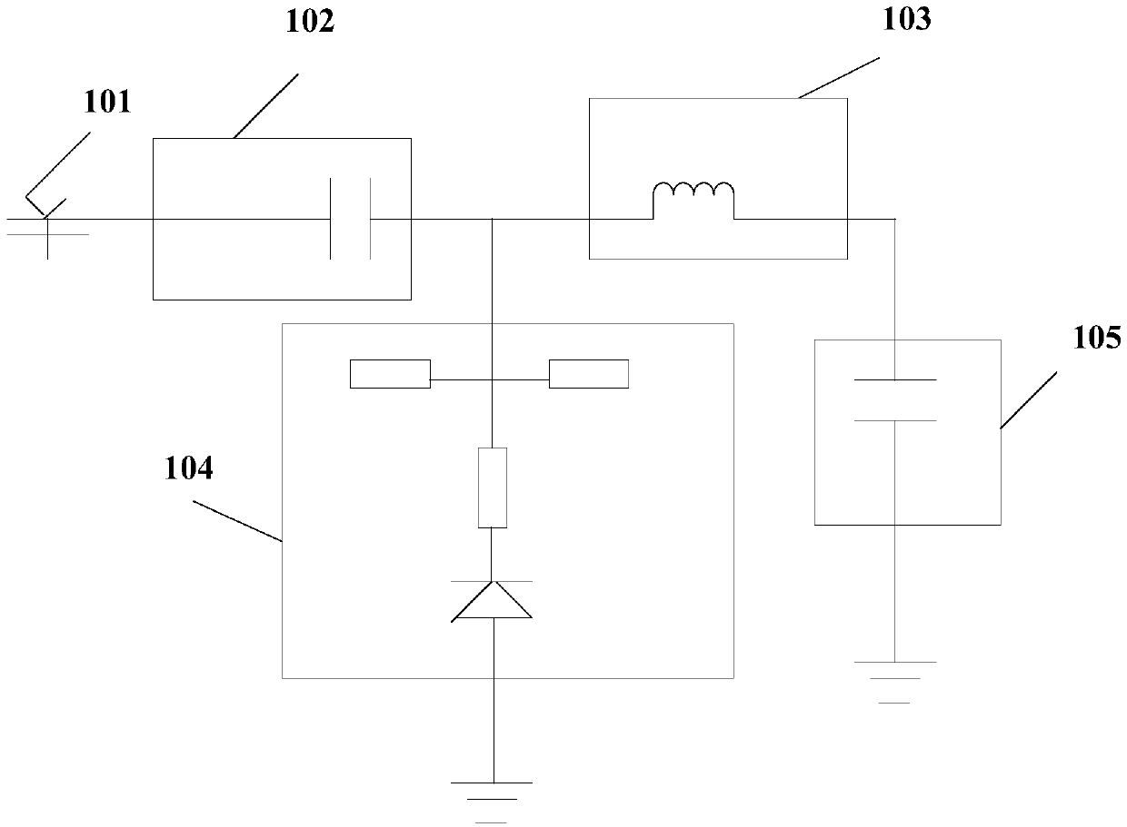
[0033] Embodiment 1 of the present application proposes a millimeter-wave rectification device oriented to single-chip implementation. In the technical solution proposed in the embodiment of the present application, the millimeter-wave rectification device is set in one chip as a whole, such as figure 1 As shown, the millimeter wave rectifying device proposed in Embodiment 1 of the present application includes an antenna 101 for receiving millimeter waves, a first isolation unit 102 , a second isolation unit 103 , a rectification unit 104 and an energy storage unit 105 .
[0034] The antenna 101 is electrically connected to the first isolation unit 102 , and the antenna is configured to receive millimeter wave energy and transmit the received millimeter wave energy to the first isolation unit 102 .
[0035] The millimeter-wave energy received by the antenna is related to the size and power of the RFID. In a preferred implementation, in the technical solution proposed in this ap...
Embodiment 2
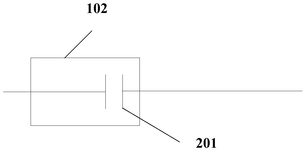
[0043] On the basis of the first embodiment above, further, the second embodiment of the present invention elaborates on the first isolation unit, as follows figure 2 As shown, the first isolation unit 102 includes at least one capacitor 201 .
[0044] Capacitor 201 is used as an energy storage element, capable of storing electric energy. The first isolation unit 201 may include multiple capacitors, or protect the capacitors through resistors, which may be determined according to the power input value of the rectifying device.
[0045] In a preferred implementation, considering the smaller size of the RFID, the first isolation unit 201 is selected to use a capacitor in the present invention, and the capacitor may be a metal-insulator-metal capacitor (MIM) capacitor, The value range of the capacitor 201 may be 0.01 picofarad to 0.2 picofarad. In the present invention, the value of the capacitor 201 is 0.1 picofarad.
[0046] Specifically, in the technical solution proposed a...
Embodiment 3
[0048] Further, on the basis of the first embodiment above, the present invention further elaborates on the second isolation unit 103, as follows image 3 As shown, the second isolation unit 103 may include at least one inductor 301 element, or other electronic components with inductive properties. No specific limitation is made here.
[0049] In this proposal, in order to adapt to the smaller size of the RFID, the second isolation unit 103 only includes an inductor 301 , and the second isolation unit 103 can further isolate the high-frequency components flowing out of the first isolation unit 102 .
[0050] Specifically, the inductance 301 can be one of layered winding inductors, and the value range of the inductance 301 is 0.1 nano-Henry to 1 nano-Henry. Preferably, in the present invention, the value of the inductance 301 is 0.5 nano-Henry. Henry.
[0051] Specifically, in the technical solution proposed by Embodiment 3 of the present invention, the inductor is a layered wi...
PUM
 Abstract
Description
Claims
Application Information


