Array substrate and micro total analysis device

An array substrate and substrate technology, applied in the detection field, can solve problems such as the inability to realize high-pixel design, increase the aspect ratio of transistor channels, etc.

Active Publication Date: 2019-04-19
BOE TECH GRP CO LTD
View PDF7 Cites 2 Cited by
  • Summary
  • Abstract
  • Description
  • Claims
  • Application Information

AI Technical Summary

Problems solved by technology

[0005] The invention provides an array substrate and a micro-full analysis device, which are used to solve the proble

Method used


Image

  • Array substrate and micro total analysis device
  • Array substrate and micro total analysis device
  • Array substrate and micro total analysis device

Examples


Embodiment Construction

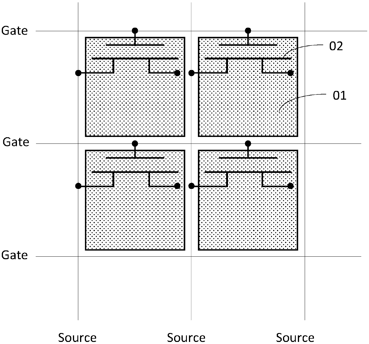
[0029] Array substrates in the related art such as figure 1 As shown, it includes a transistor located in the pixel area, the gate of the transistor is connected to the corresponding gate line Gate, the first electrode is connected to the corresponding data line Source, the second electrode is connected to the driving electrode 01, and the extension direction of the active layer pattern 02 It is arranged in parallel with the gate line Gate. In order to improve the stability of the transistor under high voltage driving, it is necessary to increase the length of the active layer pattern 02 in the extending direction. If the length of the active layer pattern 02 in the extending direction is increased, the pixel The area occupied by the region will also increase, which reduces the number of pixels disposed on the array substrate, which is not conducive to high-pixel design.

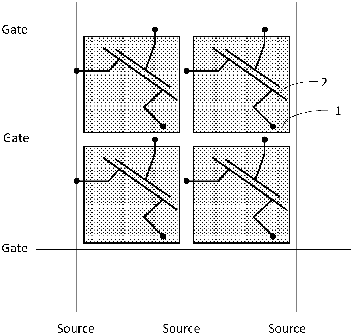
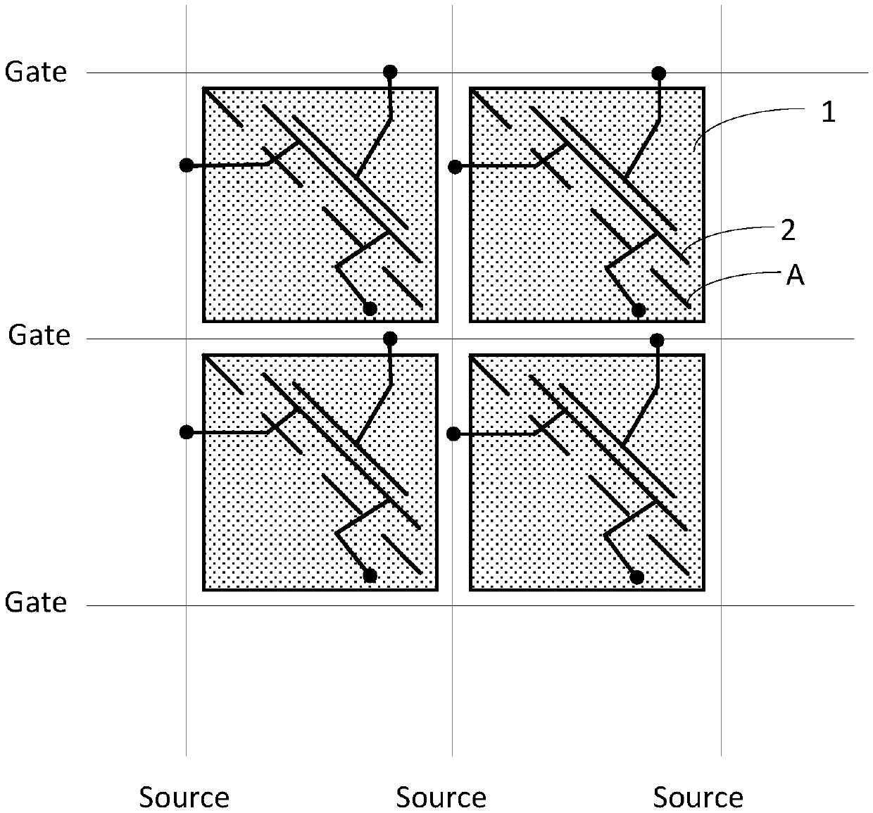
[0030] In view of the problem in the related art that increasing the channel aspect ratio of transistors ...


PUM


Abstract

The invention discloses an array substrate and a micro total analysis device. The array substrate includes a substrate, a plurality of pixel regions which are arranged on the substrate and limited bycrossing of a data line and a grid line, and driving transistors in the pixel regions, wherein each driving transistor includes an active layer graph, and a first preset angle is displayed between theextending direction of the active layer graph and the grid line, and the active layer graph strides the pixel region in an inclined manner in the first preset angle direction; and the source and drain electrodes of each driving transistor are connected to the active layer graph in the first preset angle direction. By setting the first preset angle between the extending direction of active layer graph and the grid line, compared with a conventional device which sets the extending direction of the active layer to be parallel with the grid line, the array substrate can increase the length of theactive layer graph in the extending direction, thus increasing the length breadth ratio of the active layer graph while not increasing the area of the occupied pixel area, so as to improve the conductivity of the driving transistors while realizing high pixel design.

Description

technical field [0001] The invention relates to the technical field of detection, in particular to an array substrate and a micro-total analysis device. Background technique [0002] The conduction capability of the transistors on the array substrate directly affects the accuracy of data transmission. Especially as the driving voltage increases, the stability of the transistor will be greatly affected. That is, as the voltage increases, the threshold voltage and characteristics of the transistor will become poor, thereby affecting the conduction characteristics of the transistor. [0003] In related technologies, by increasing the aspect ratio of the active layer pattern of the transistor, the stability of the transistor can be improved, and the conduction characteristics of the transistor can also be guaranteed to be unaffected when the driving voltage is increased, but increasing the active layer of the transistor The aspect ratio of the graphics will occupy a larger are...

Claims


Application Information

Patent Timeline
IPC IPC(8): H01L27/12G01N21/27
CPCH01L27/1222G01N21/27H01L27/124B01L2300/168B01L3/502792B01L2400/0427G01N21/255G02F1/13624H10K59/1213
Inventor 刘英明董学王海生陈小川丁小梁王雷李昌峰顾品超张平曹学友
Owner BOE TECH GRP CO LTD
Why Eureka
Try Eureka