Schottky diode and preparation method thereof

A Schottky diode and anode technology, applied in semiconductor/solid-state device manufacturing, electrical components, circuits, etc., can solve the problem of difficult P-type injection, low breakdown voltage and conduction characteristics of Schottky diodes, and reduced potential barriers and other problems, to achieve the effect of improving the breakdown characteristics and conduction characteristics, improving the fringe electric field, and increasing the contact area.

Pending Publication Date: 2020-05-12
THE 13TH RES INST OF CHINA ELECTRONICS TECH GRP CORP
View PDF9 Cites 2 Cited by
  • Summary
  • Abstract
  • Description
  • Claims
  • Application Information

AI Technical Summary

Problems solved by technology

However, due to the deep acceptor level of gallium oxide, there is a hole self-confinement effect, and the potential barrier is reduced due to the influence of the image force, and the P-type injection is extremely difficul

Method used


Image

  • Schottky diode and preparation method thereof
  • Schottky diode and preparation method thereof
  • Schottky diode and preparation method thereof

Examples


Embodiment Construction

[0044] In order to make the object, technical solution and advantages of the present invention more clear, the present invention will be further described in detail below with reference to the accompanying drawings and in combination with the embodiments. It should be understood that the specific embodiments described here are only used to explain the present invention, not to limit the present invention.

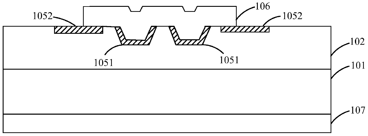
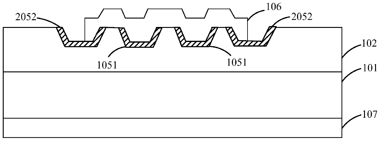
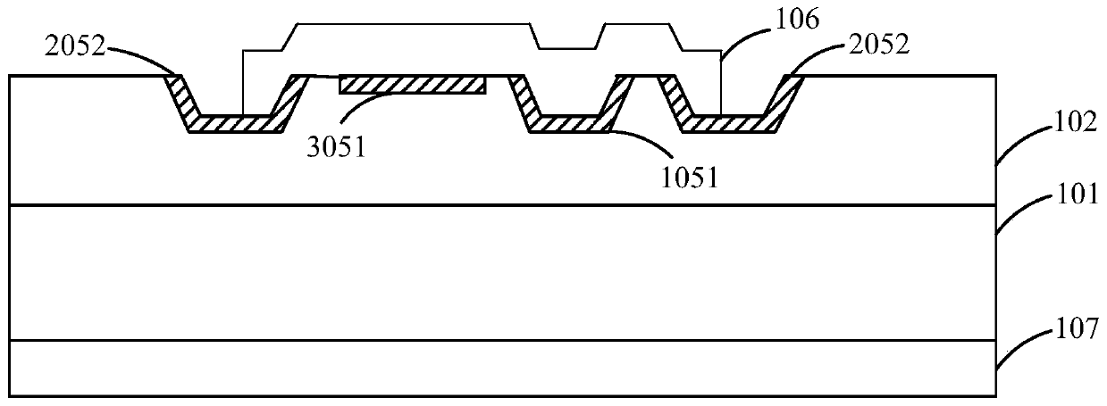
[0045] figure 1 It is a schematic diagram of the cross-sectional structure of the Schottky diode provided by the embodiment of the present invention, referring to figure 1 , the Schottky diode can consist of:

[0046] Substrate 101;

[0047] An n-type gallium oxide layer 102 is formed on the substrate 101, wherein the n-type gallium oxide layer 102 includes: at least one first thermal oxidation region 1051 and two second thermal oxidation regions 1052;

[0048] An anode metal layer 106 is formed on the n-type gallium oxide layer 102, wherein the area corresponding to the...


PUM


Abstract

The invention relates to the field of semiconductors, in particular to a Schottky diode and a preparation method thereof. The Schottky diode comprises: a substrate; an n-type gallium oxide layer formed on the substrate, wherein the n-type gallium oxide layer comprises at least one first thermal oxidation region and two second thermal oxidation regions; an anode metal layer which is formed on the n-type gallium oxide layer; the first thermal oxidation region located below the anode metal layer, wherein the second thermal oxidation regions are partially located below the anode metal layer; a cathode metal layer which is formed on the back surface of the substrate, wherein at least one first thermal oxidation region is provided with a groove structure. Compared with an existing Schottky diode, the Schottky diode has the advantages that the electric field at the anode junction is better, and the high-voltage resistance characteristic and the conduction characteristic are better.

Description

technical field [0001] The invention relates to the field of semiconductors, in particular to a Schottky diode and a preparation method thereof. Background technique [0002] At present, the most widely used semiconductor silicon material has many advantages, including its simple substance / oxide interface is easy to obtain, the doping and diffusion process is relatively mature, the earth's reserves are large, and the cost of raw materials is low. However, due to the electrons and holes of silicon itself Due to the limitation of migration speed, its application in high-power semiconductor devices is limited; and gallium nitride material, which is a representative of the third-generation semiconductor, has a breakdown resistance due to its wide band gap and high thermal conductivity. High voltage, high operating temperature and strong radiation resistance are ideal high-power semiconductor materials. However, the preparation process is complicated and the preparation cost is h...

Claims


Application Information

Patent Timeline
IPC IPC(8): H01L29/872H01L29/06H01L21/335
CPCH01L29/872H01L29/0603H01L29/0615H01L29/0684H01L29/66143
Inventor 王元刚吕元杰冯志红刘红宇梁士雄宋旭波周幸叶谭鑫郭红雨
Owner THE 13TH RES INST OF CHINA ELECTRONICS TECH GRP CORP
Why Eureka
Try Eureka