Vertical high-voltage MOSFET device and manufacturing method thereof

A vertical, device technology, applied in the field of microelectronics, can solve the problems of increasing the difficulty of etching and masking, limiting the etching depth, and increasing static power consumption, so as to reduce the difficulty of masking and etching, and reduce the static power consumption. Power consumption and the effect of reducing reverse leakage

Active Publication Date: 2019-08-13
XIDIAN UNIV
View PDF4 Cites 3 Cited by
  • Summary
  • Abstract
  • Description
  • Claims
  • Application Information

AI Technical Summary

Problems solved by technology

At present, the horizontal gallium oxide MOSFET device with a breakdown voltage of 750V and the vertical gallium oxide MOSFET device with a breakdown voltage of 185V have been realized. The gate of this vertical gallium oxide MOSFET device is directly written by an electron beam. It is etched after the mold, the distance between adjacent gates is 200-400nm, the gate width is about 400nm, and the gate length is about 500nm. The small mask size increases the difficulty of etching and masking, and limits the etching Depth, which limits the breakdown voltage, and the masking method of electron beam direct writing is costly
Since gallium oxide only has n-type materials at present, it is difficult to realize p-type materials. The above-mentioned vertical gallium oxide MOSFET device can only be turned off by applying a negative gate voltage. In practical applications, an additional power supply needs to be configured for it, which increases static power consumption.

Method used


Image

  • Vertical high-voltage MOSFET device and manufacturing method thereof
  • Vertical high-voltage MOSFET device and manufacturing method thereof

Examples


Embodiment 1

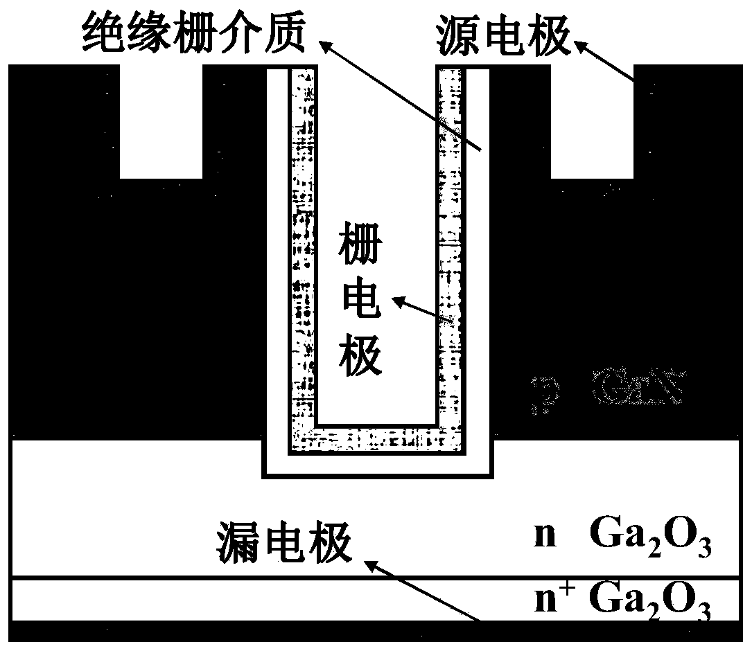
[0040] Embodiment 1, make substrate front electron density be 10 15 cm -3 , the hole concentration of the p-type GaN epitaxial layer is 10 17 cm -3 vertical high voltage MOSFET devices.

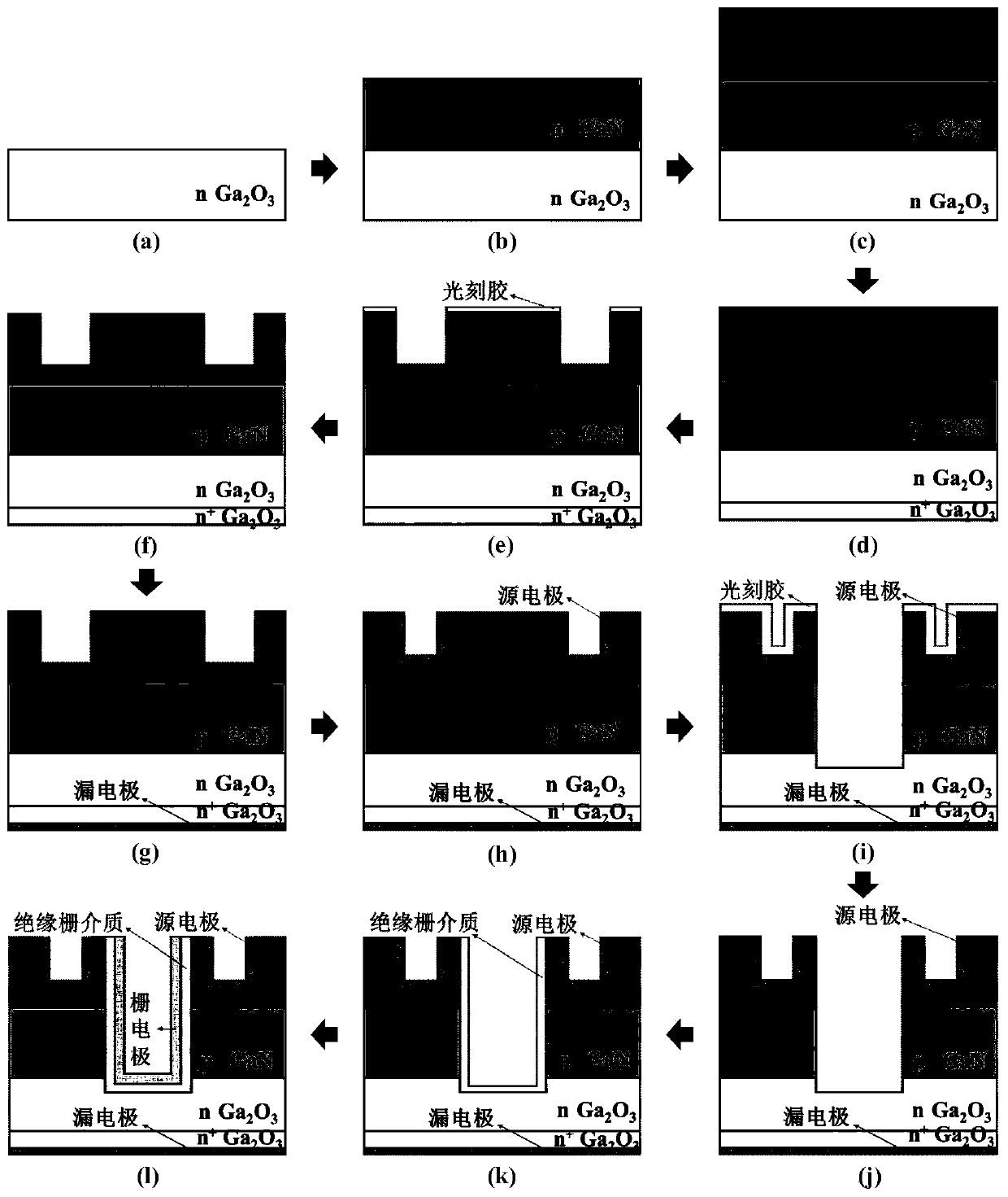
[0041] Step 1, carry out organic cleaning to substrate, such as figure 2 (a).

[0042] Use n-type Ga 2 o 3 The substrate was cleaned with flowing deionized water, and then placed in HF:H 2 Corrosion was carried out in the solution of O=1:1 for 30-60s, and finally cleaned with flowing deionized water and dried with high-purity nitrogen.

[0043] Step 2, growing a p-type GaN epitaxial layer on the substrate, such as figure 2 (b).

[0044] Will clean the Ga 2 o 3 Put the substrate into the reaction chamber of the MOVPE equipment, set the pressure of the reaction chamber at 80Torr, the temperature at 600°C, and at the same time feed NH at a flow rate of 800sccm 3 , with a flow rate of 800sccm of trimethylgallium, a 300nm thick GaN film was grown by vapor phase epitaxy; and then anne...

Embodiment 2

[0065] Embodiment 2, making the electron concentration on the front side of the substrate is 5×10 15 cm -3 , the hole concentration in the p-type GaN epitaxial layer is 5×10 17 cm -3 vertical high voltage MOSFET devices.

[0066] Step 1, the substrate is organically cleaned, such as figure 2 (a).

[0067] The specific implementation method of this step is the same as step 1 in embodiment 1;

[0068] Step 2, growing a p-type GaN epitaxial layer on the substrate, such as figure 2 (b).

[0069] Will clean the Ga 2 o 3 The substrate is placed in the reaction chamber of the MOVPE equipment, and a 400nm thick GaN film is grown by vapor phase epitaxy, and then annealed at a temperature of 100°C for 150s to obtain a sample with p-type GaN on the substrate. The process conditions are as follows :

[0070] Set the pressure of the reaction chamber at 100 Torr, the temperature at 700°C, and at the same time feed NH at a flow rate of 1000 sccm 3 , trimethylgallium at a flow ra...

Embodiment 3

[0096] Embodiment 3, make substrate front electron density be 10 16 cm -3 , the hole concentration of the p-type GaN epitaxial layer is 10 18 cm -3 vertical high voltage MOSFET devices.

[0097] Step A, carry out organic cleaning to substrate, as figure 2 (a).

[0098] The specific implementation method of this step is the same as step 1 in embodiment 1;

[0099] Step B, growing a p-type GaN epitaxial layer on the substrate, such as figure 2 (b).

[0100] Will clean the Ga 2 o 3 Put the substrate into the reaction chamber of the MOVPE equipment, set the pressure of the reaction chamber at 150 Torr, and the temperature at 800°C, and simultaneously feed NH with a flow rate of 1400 sccm into the reaction chamber 3 , trimethylgallium with a flow rate of 1400sccm, and a 500nm thick GaN film grown by vapor phase epitaxy;

[0101] Then annealed at a temperature of 1100° C. for 180 s to obtain a sample with p-type GaN growing on the substrate.

[0102] Step C, growing n-t...


PUM


Abstract

The invention discloses a vertical high-voltage MOSFET device and a manufacturing method thereof, and mainly solves the problems that a vertical MOSFET device in the prior art is low in breakdown voltage and is large in leakage current. The device comprises a drain electrode, a substrate and epitaxial layers from bottom to top, wherein shallow grooves with the depth being less than 300 nm is formed in the surface of the upper epitaxial layer. A source electrode is arranged in the shallow grooves, and deep grooves which are greater than 500 nm in depth and penetrate through the two epitaxial layers to the surface of the substrate are formed between the shallow grooves in the surface of the upper epitaxial layer; insulated gate media and gate electrodes are arranged in the deep grooves, andthe substrate is made of n-type Ga2O3 materials, wherein the number of the epitaxial layers is two, and the materials are sequentially p-type GaN with the hole concentration of 1,017-1018cm<-3> and n-type Ga2O3 with the electron concentration of 1,018-1019cm<-3> from bottom to top in sequence. The device improves the breakdown voltage, reduces the reverse leakage and static power consumption, reduces the manufacturing cost and difficulty, and can be used for power devices and high-voltage switching devices.

Description

technical field [0001] The invention belongs to the technical field of microelectronics and relates to a vertical semiconductor device, which can be used for power devices and high-voltage switching devices. Background technique [0002] The horizontal MOSFET device is an easy-to-implement device structure, and the device performance of the first-generation semiconductor materials represented by silicon materials has been difficult to meet the current development needs. In order to reduce the scale of integrated circuits and improve the performance of devices, it can be improved from two aspects of device structure and materials. Gallium oxide, as a wide bandgap semiconductor material, has five isomers, of which monoclinic β-type Ga 2 o 3 The stability is the best, the bandgap width is about 4.8eV-4.9eV, and the theoretical breakdown electric field can reach 8MV / cm, which is twice more than the other two excellent wide bandgap semiconductor materials, silicon carbide and g...

Claims


Application Information

Patent Timeline
Patent Type & Authority Applications(China)
IPC IPC(8): H01L29/78H01L29/06H01L29/20H01L29/24H01L21/336
CPCH01L29/7813H01L29/0623H01L29/0638H01L29/2003H01L29/24H01L29/66727H01L29/66734H01L29/267H01L29/41766
Inventor 冯倩蔡云匆封兆青胡壮壮张春福周弘张进成
Owner XIDIAN UNIV
Why Eureka
Try Eureka