Semiconductor device and preparation method thereof
A semiconductor and nitride semiconductor technology, used in semiconductor devices, semiconductor/solid-state device manufacturing, electrical components, etc., can solve problems such as inability to achieve simultaneous realization, achieve good channel regulation capability, low reverse leakage, and simple process. Effect
- Summary
- Abstract
- Description
- Claims
- Application Information
AI Technical Summary
Problems solved by technology
Method used
Image
Examples
Embodiment 1
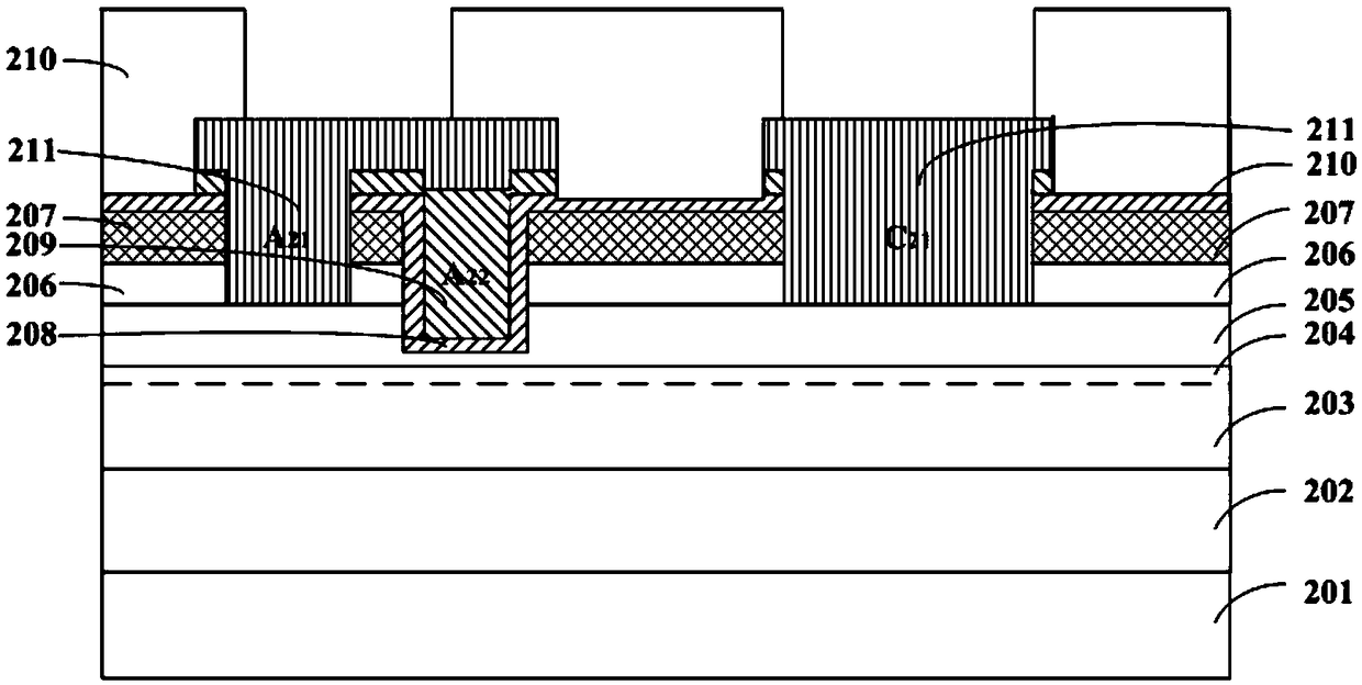
[0063] Please refer to figure 2 , a schematic cross-sectional structure of a semiconductor device given in this embodiment, specifically including a buffer layer 202 , a channel layer 203 , a barrier layer 205 , a cap layer 206 , a passivation layer 207 , and a dielectric layer that are sequentially generated on the substrate 201 208 , anode metal 209 and protective layer 210 .
[0064] Wherein, the anode of the semiconductor device includes the first anode A 21 and the second anode A 22 , the cathode of the semiconductor device is the cathode C 21 .
[0065] Specifically, the substrate 201 can be prepared by using common substrate materials such as GaN, SiC or Si, and its thickness is set according to actual needs. The buffer layer 202 may be composed of one or more combinations of superlattice, AlN, and AlGaN. The channel layer 203 can be made of GaN and has a thickness of 3-5 μm. The barrier layer 205 can be made of Al x Ga 1-x N,In x Ga 1-x N,In x Al 1-x N, an...
Embodiment 2
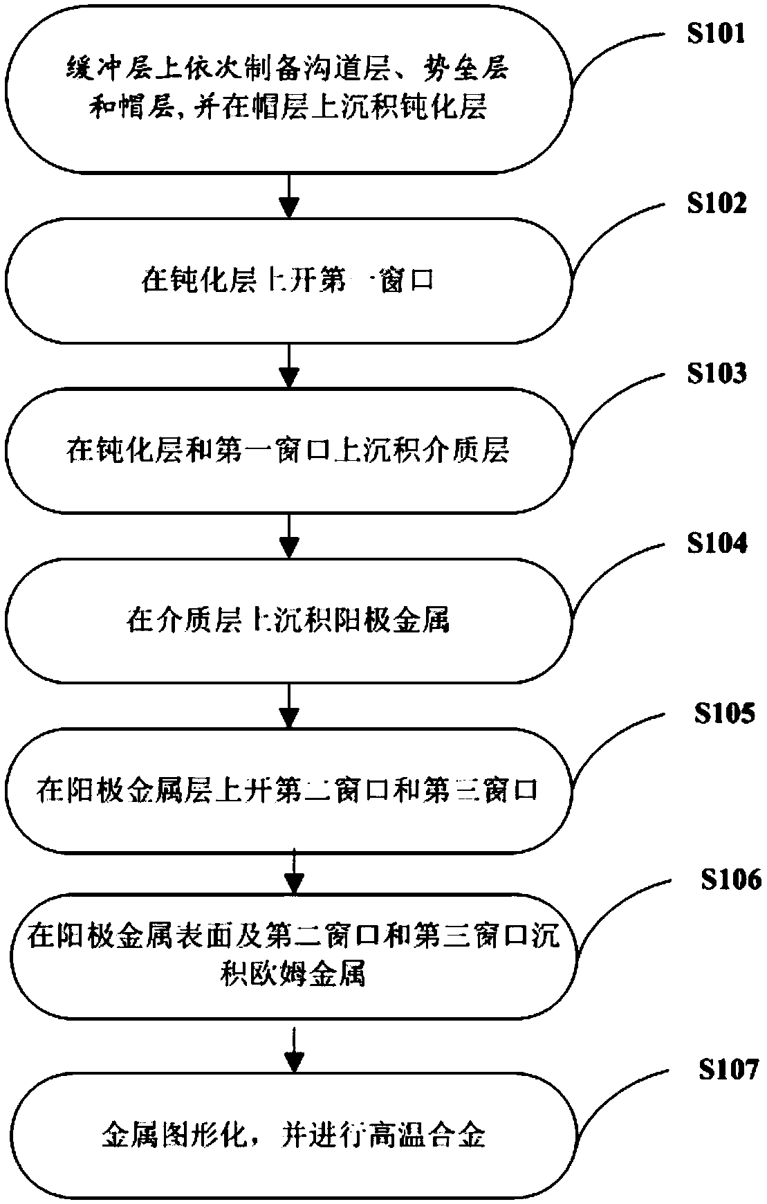
[0070] Based on the description of the above embodiments, the present invention also provides a method for preparing the above semiconductor device, such as image 3 shown, including the following steps:
[0071] S101, preparing a buffer layer, a channel layer, a barrier layer and a cap layer in sequence on the substrate, and depositing a passivation layer on the cap layer;
[0072] S102 , opening a first window on the passivation layer, and the bottom of the first window is located on the barrier layer or inside the barrier layer.
[0073] S103, a dielectric layer is prepared on the passivation layer and the first window.
[0074] S104, depositing an anode metal layer on the dielectric layer. Thus, a MIS junction structure composed of a dielectric layer separating the anode metal layer and the barrier layer is formed in the first window, that is, the second anode electrode of the semiconductor device. Wherein, the anode metal can be composed of at least one of TiN, Ni, Au, W...
Embodiment 3
[0100] Further, as another improvement of the previous embodiment, as Figure 5 As shown, it is a schematic diagram of the cross-sectional structure of the SBD, which specifically includes a buffer layer 402, a channel layer 403, a barrier layer 405, a cap layer 406, a passivation layer 407, a dielectric layer 408, and an anode metal 409 that are sequentially generated on the substrate 401. and protective layer 410.
[0101] Wherein, the anode of the semiconductor device includes the first anode A 31 and the second anode A 32 , the cathode of the semiconductor device is the cathode C 31 .
[0102] Specifically, the substrate 401 can be prepared by using common substrate materials such as GaN, SiC, or Si, and its thickness is set according to actual needs. The buffer layer 402 may be composed of one or more combinations of superlattice, AlN, and AlGaN. The channel layer 403 can be made of GaN and has a thickness of 3-5 μm. The barrier layer 405 can be made of Al x Ga 1-...
PUM
 Abstract
Description
Claims
Application Information


