Silicon chip identification method
A technology for silicon wafers and silicon wafer boxes, applied in the field of silicon wafer identification, can solve problems such as inconvenience, and achieve the effects of improving utilization, reducing the risk of errors, and reducing usage
- Summary
- Abstract
- Description
- Claims
- Application Information
AI Technical Summary
Problems solved by technology
Method used
Image

Examples
Embodiment Construction
[0031] The core idea of the present invention is that the present invention provides a silicon chip identification method, comprising the following steps:
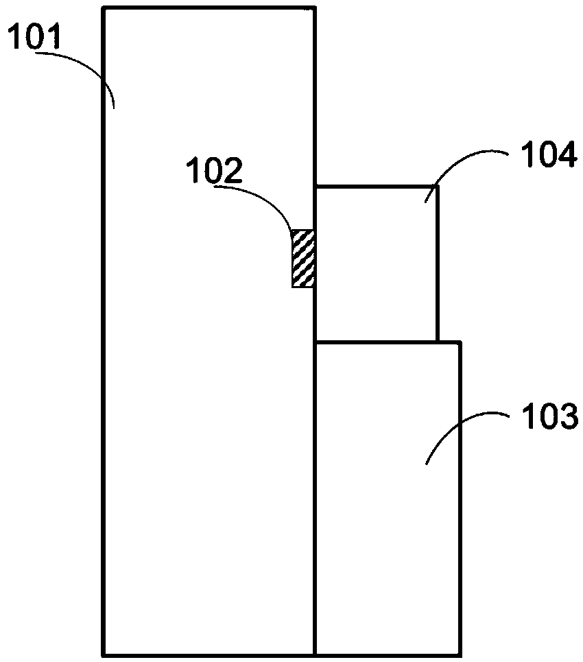
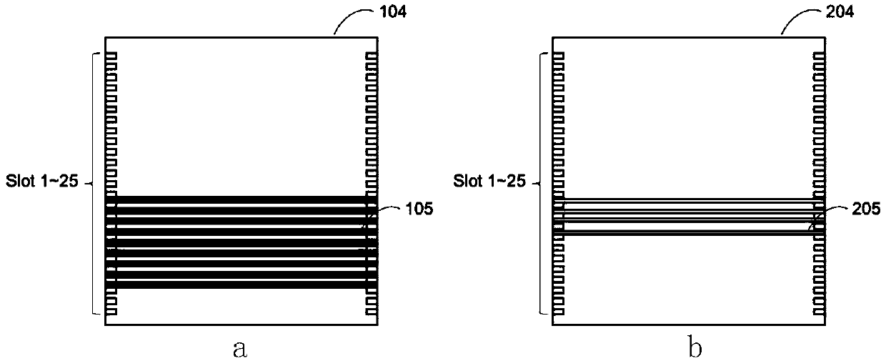
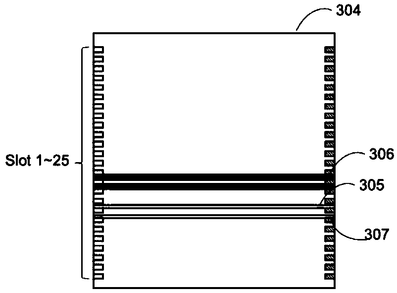
[0032] Step S01: Using a silicon wafer box, after the silicon wafers are picked and placed, scan the ID information of the silicon wafers to be identified at each slot position in the silicon wafer box to obtain the IDs of all the silicon wafers to be identified in the silicon wafer box information;
[0033] Step S02: Transfer the ID information of the silicon wafer to be identified to the manufacturing execution system;
[0034] Step S03: comparing the ID information of the silicon wafer to be identified by the manufacturing execution system to confirm the type of the silicon wafer to be identified. May also include:
[0035] Step S04: Through the manufacturing execution system, the ID information of the silicon wafer to be identified after the type is confirmed is transmitted in real time to the equipment that needs ...
PUM
 Abstract
Description
Claims
Application Information
 - R&D Engineer
- R&D Manager
- IP Professional
- Industry Leading Data Capabilities
- Powerful AI technology
- Patent DNA Extraction
Browse by: Latest US Patents, China's latest patents, Technical Efficacy Thesaurus, Application Domain, Technology Topic.
© 2024 PatSnap. All rights reserved.Legal|Privacy policy|Modern Slavery Act Transparency Statement|Sitemap