DC offset compensation system and method

A DC offset and compensation system technology, applied in the transmission system, electrical components, etc., can solve the problems of low compensation accuracy, complex analog negative feedback scheme circuit, poor stability, etc., to improve compensation accuracy, reduce power consumption and area, The effect of increasing the compensation speed

Active Publication Date: 2019-04-23
SANECHIPS TECH CO LTD
View PDF6 Cites 1 Cited by
  • Summary
  • Abstract
  • Description
  • Claims
  • Application Information

AI Technical Summary

Problems solved by technology

Because the AC coupling technology is difficult to apply in the zero-IF receiver, the circuit of the analog negative feedback scheme in the DC negative feedback is complex and the stability is poor, and the circuit of the digital negative feedback scheme in the DC negative feedback is simple; therefore, the zero-IF receiver Usually a digital negative feedback scheme is used to compensate the DC offset
However, the digital negative feedback scheme will be limited by the performance of the DC offset compensation system when compensating the DC offset, resulting in low compensation accuracy

Method used


Image

  • DC offset compensation system and method
  • DC offset compensation system and method
  • DC offset compensation system and method

Examples


Embodiment Construction

[0054] It can be seen from the background art that the DC offset compensation scheme in the related art has the problem of low compensation accuracy when compensating the DC offset of the receiver.

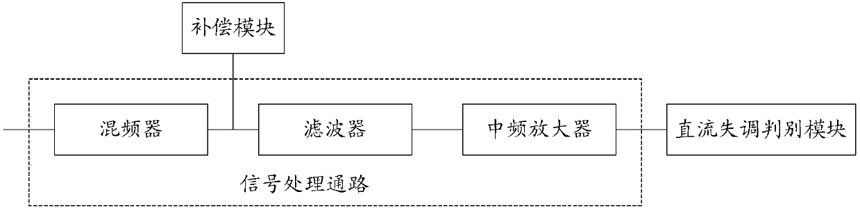
[0055] E.g, figure 1 It is a schematic diagram of the structure of the DC offset compensation system based on the AC coupling scheme, from figure 1 It can be seen that the receiver contains a signal processing path, which includes a mixer, a filter, and an intermediate frequency amplifier; a DC blocking capacitor can be added to the signal processing path to compensate for the DC offset. However, the large number of discrete capacitors required by this solution and the large size of the required capacitors make it impractical to integrate these capacitors, making the AC-coupling scheme difficult to implement in zero-IF receivers.

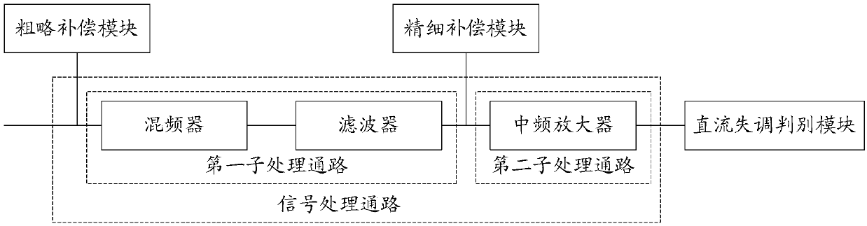
[0056] figure 2 is a schematic diagram of the structure of a single-channel DC offset compensation system based on a digital negative feedback schem...


PUM


Abstract

The invention discloses a DC offset compensation system, comprising: a signal processing circuit, a first compensation module, a second compensation module and a third compensation module. The first compensation module is configured to compensate a DC offset of a second sub-processing circuit in the signal processing circuit, so that a first DC offset value output by the signal processing circuitis less than or equal to a first threshold; the second compensation module is configured to compensate the DC offset of a first sub-processing circuit based on the first DC offset value, so that a second DC offset value output by the signal processing circuit is less than or equal to a second threshold; and the third compensation module is configured to compensate the DC offset of the signal processing circuit based on the second DC offset value, so that a third DC offset value output by the signal processing circuit is less than or equal to a third threshold. The invention further discloses aDC offset compensation method.

Description

technical field [0001] The invention relates to receiver technology of wireless communication, in particular to a direct current offset compensation system and method. Background technique [0002] In recent years, wireless communication technology has developed rapidly, and devices with wireless communication functions, such as smart phones, tablet computers, and notebook computers, have become more and more widely used, which greatly facilitates people's daily work and life. People's demand for the portability of wireless devices makes low power consumption and high integration become more and more important in the design of wireless transceivers; and in wireless transceivers, the design of the receiver is often the key. [0003] Among common wireless receiver structures, zero-IF receivers have great advantages in low power consumption and high integration, and are very suitable for application in today's wireless devices. However, since the IF signal of the zero-IF recei...

Claims


Application Information

Patent Timeline
Patent Type & Authority Applications(China)
IPC IPC(8): H04B1/30
CPCH04B1/30H04B2001/305
Inventor 吴毅强裴斐
Owner SANECHIPS TECH CO LTD
Why Eureka
Try Eureka