Semiconductor wafer grinding device with cleaning function

A grinding device and cleaning device technology, which is applied in the direction of grinding devices, semiconductor/solid-state device manufacturing, grinding machine tools, etc., can solve the problems that affect the service life of grinding discs, cannot handle sludge, and fix wafers, etc., so as to improve the service life, Easy to disassemble and contribute to the effect of grinding

Active Publication Date: 2019-04-26
JIANGSU NEPES SEMICON
View PDF8 Cites 5 Cited by
  • Summary
  • Abstract
  • Description
  • Claims
  • Application Information

AI Technical Summary

Problems solved by technology

[0003] Chinese patent (authorized announcement number: CN207495157U) discloses a semiconductor wafer thinning device, including a thinning device, a unit box is arranged on the lower side of the thinning device, and a lifting platform is fixedly installed on the upper surface of the unit box. A fixed plate is arranged on the upper side of the lifting platform, and an adsorption platform is fixedly installed on the surface of the fixed plate. Left and right braces are arranged on both sides of the unit box, and the unit box and the control cabinet are fixed by the right brace. connection, the top of the left strut and the right strut is fixedly installed with a crossbeam, a fixed block is arranged in the middle of the crossbeam, a hydraulic shaft is arranged inside the fixed block, and a rotating shaft plate is fixedly installed at the lower end of the hydraulic shaft, but the above device It cannot handle the sludge accumulated between the grinding disc and the fixing device, which affects the service life of the grinding disc. At the same time, the above-mentioned device cannot fix the side of the wafer, so that the wafer has a risk of side slipping. Therefore, in view of the above situation , there is an urgent need to develop a semiconductor wafer grinding device with cleaning function to overcome the deficiencies in current practical applications

Method used


Image

  • Semiconductor wafer grinding device with cleaning function
  • Semiconductor wafer grinding device with cleaning function
  • Semiconductor wafer grinding device with cleaning function

Examples


Embodiment 1

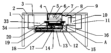
[0026] see Figure 1~4 , in an embodiment of the present invention, a semiconductor wafer grinding device with a cleaning function includes a support rod 1, a top plate 2, a cleaning device 16 and a fixing device 33, and support rods 1 are provided on both sides of the bottom of the top plate 2, and the The support rod 1 is fixedly connected with the top plate 2, the inner side of the support rod 1 is provided with a connecting rod 3 fixedly connected with the top plate 2, the inner side of the connecting rod 3 is provided with a fixing seat 34, and the top of the fixing seat 34 is provided with a fixing device 33 , the upper side of the fixing device 33 is provided with a motor 6, the motor 6 is fixedly connected to the top plate 2, the output end of the lower side of the motor 6 is connected to the grinding disc 7, and the outer side of the grinding disc 7 is provided with a cleaning device 16, so The cleaning device 16 is fixedly connected with the fixing base 34 .

[0027...

Embodiment 2

[0031] A grinding device, comprising the semiconductor wafer grinding device with cleaning function described in Embodiment 1.

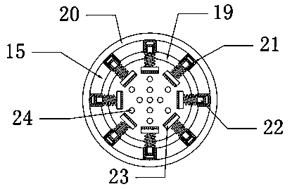
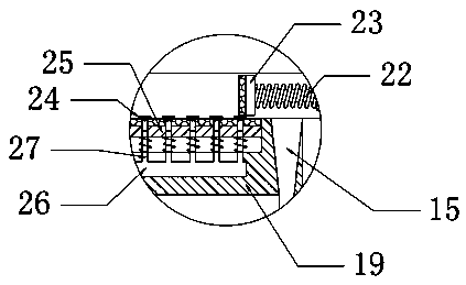
[0032] The semiconductor wafer grinding device with cleaning function can realize longitudinal absorption and fixation of the wafer by setting the first fixing block 19, and can carry out lateral extrusion and fixing of the wafer by setting the second fixing block 20, effectively reducing the The circle may slip during grinding. The coarse grinding teeth 30 and the fine grinding teeth 31 are made of diamond, which can improve the service life of the grinding teeth. By setting the coarse grinding teeth 30 and the fine grinding teeth 31, the grinding disc can be used Coarse grinding can also be finely ground, which is conducive to improving the grinding quality. By setting the elbow 14, the fine dust generated during the grinding process can be absorbed, so that water resources can be recycled. By setting the cleaning device 16, it can be cleaned during...


PUM


Abstract

The invention relates to the technical field of grinding equipment, in particular to a semiconductor wafer grinding device with the cleaning function. The semiconductor wafer grinding device comprisessupporting rods, a top plate, a cleaning device and a fixing device. The supporting rods are arranged on the two sides of the bottom of the top plate. The inner sides of the supporting rods are provided with connecting rods. A fixed seat is arranged on the inner sides of the connecting rods. The fixing device is arranged on the top of the fixed seat. A motor is arranged on the upper side of the fixing device. The output end of the lower side of the motor is connected with a grinding disk. The cleaning device is arranged on the outer side of the grinding disk. The semiconductor wafer grindingdevice is provided with the fixing device, and the probability of side slipping of wafers in the grinding process is effectively reduced. The grinding quality can be improved through arrangement of rough grinding teeth and fine grinding teeth. The grinding disk and a first fixing block can be kept clean through the cleaning device. Through frequent cleaning, the grinding disk can be kept clean. Meanwhile, in the cleaning process, cleaning water can serve as cooling water for grinding silicon wafers to facilitate grinding on the silicon wafers.

Description

technical field [0001] The invention relates to the technical field of grinding equipment, in particular to a semiconductor wafer grinding device with a cleaning function. Background technique [0002] Wafer refers to the silicon wafer used in the production of silicon semiconductor integrated circuits. Because of its circular shape, it is called a wafer; it can be processed into various circuit element structures on the silicon wafer, and become an IC with specific electrical functions. Products, wafers need to be ground when they are put into use. [0003] Chinese patent (authorized announcement number: CN207495157U) discloses a semiconductor wafer thinning device, including a thinning device, a unit box is arranged on the lower side of the thinning device, and a lifting platform is fixedly installed on the upper surface of the unit box. A fixed plate is arranged on the upper side of the lifting platform, and an adsorption platform is fixedly installed on the surface of t...

Claims


Application Information

Patent Timeline
Patent Type & Authority Applications(China)
IPC IPC(8): B24B37/10B24B37/30B24B37/34H01L21/67
CPCB24B37/10B24B37/30B24B37/34H01L21/6704H01L21/67092
Inventor 汪文坚王倩朱威莉
Owner JIANGSU NEPES SEMICON
Why Eureka
Try Eureka