

Asymmetrical lens and optical devices
An asymmetric and optical device technology, applied in the direction of lenses, optical components, optics, etc., can solve the problems of low versatility of lenses and unfavorable automatic production, and achieve the effect of being conducive to large-scale automatic production and high versatility
- Summary
- Abstract
- Description
- Claims
- Application Information
AI Technical Summary
Problems solved by technology
Method used
Image

Examples
Embodiment 1
[0051] Embodiment 1 of the present invention provides an asymmetric lens, such as Figure 4 to Figure 5 As shown, it includes a first light-transmitting surface 41, a second light-transmitting surface 42 and a lens carrier 43;
[0052] The second light-transmitting surface 42 is a body of revolution with the center of the optical axis 44 as the axis;
[0053] The first light passing surface 41 is arranged on one side of the lens carrier 43, and the second light passing surface 42 is arranged on the other side of the lens carrier 43 opposite to the first light passing surface 41;
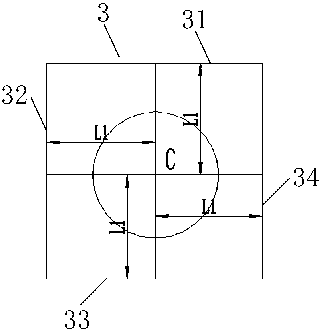
[0054] The optical axis center 44 deviates from the geometric center of the lens carrier 43 by a preset distance.
[0055] The present invention adopts an asymmetric lens, the optical axis center of the asymmetric lens deviates from the geometric center of the lens carrier by a preset distance, and the optical axis center and each coupling surface of the lens carrier differ by a preset vertical distan...
Embodiment 2
[0060] Embodiment 2 of the present invention provides an optical device, see Image 6 , including the asymmetric lens 4, the optical device chip 5, the heat sink 6 and the optical circuit substrate 7 described in any one of the first embodiment of the present invention;
[0061] The heat sink 6 is arranged on the optical path substrate 7, and the optical device chip 5 is arranged on the heat sink 6;
[0062] The asymmetric lens 4 is arranged on the optical path substrate 7, the asymmetric lens 4 is coupled with the optical path substrate 7, and the cured glue is filled between the two;
[0063] Wherein, the asymmetric lens 4 is selected for the coupling surface with the optical circuit substrate 7, based on the sum of the distance between the coupling surface and the optical axis center 44 and the thickness of the filled and cured glue, and the optical device chip 5 The height of the light outlet or the light inlet is determined to be the same, and the selected distance betwe...
Embodiment 3
[0077] Embodiment 3 of the present invention provides an optical device, such as Figure 11 As shown, it includes the asymmetric lens 4, the optical device chip 5, the heat sink 6 and the optical circuit substrate 7 described in any one of the first embodiment of the present invention;
[0078] The heat sink 6 is arranged on the optical path substrate 7, and the optical device chip 5 is arranged on the heat sink 6;
[0079] The asymmetric lens 4 is disposed on the optical path substrate 7 , and the optical axis center 44 of the asymmetric lens 4 is coupled to the light exit port or the light entry port of the optical device chip 5 .
[0080] The present invention uses an asymmetric lens, the center of the optical axis of the asymmetric lens deviates from the geometric center of the lens carrier by a preset distance, and the distances between the center of the optical axis and the bearing surfaces of the lens carrier differ by a preset distance. Assuming a vertical distance, a...
PUM
 Abstract
Description
Claims
Application Information