Scintillation screen packaging structure manufacturing method, scintillation screen packaging structure and image detector

A technology of packaging structure and manufacturing method, applied in the field of X-ray radiation imaging, can solve the problems of X-ray overflow, low absorption efficiency, harmful electronic circuits, etc., and achieve the effect of improving X-ray absorption rate and reducing radiation interference

Active Publication Date: 2020-12-11
NANOVISION TECHNOLOGY (BEIJING) CO LTD
View PDF6 Cites 0 Cited by
  • Summary
  • Abstract
  • Description
  • Claims
  • Application Information

AI Technical Summary

Problems solved by technology

Therefore, the columnar scintillation screen will cause X-ray overflow due to low absorption efficiency, which is harmful to the electronic circuit in the underlying photosensitive device

Method used


Image

  • Scintillation screen packaging structure manufacturing method, scintillation screen packaging structure and image detector
  • Scintillation screen packaging structure manufacturing method, scintillation screen packaging structure and image detector
  • Scintillation screen packaging structure manufacturing method, scintillation screen packaging structure and image detector

Examples


Embodiment Construction

[0040] The technical content of the present invention will be further described in detail below in conjunction with the accompanying drawings and specific embodiments.

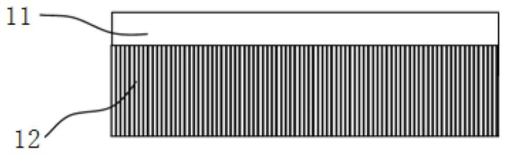
[0041] In the present invention, the scintillation screen packaging structure refers to the crystal columnar scintillation screen packaging structure, which is used to convert the incident X-rays into visible light and transmit them to the X-ray image sensor, so that the X-ray image The electronic circuit in the sensor and X-ray image sensor converts the received visible light into an analog signal, converts it into a digital signal through an A / D converter (analog / digital converter), and transmits it to the computer to obtain the initial digital image of the X-ray.

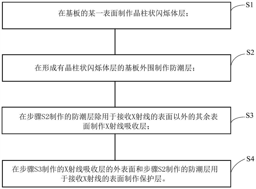
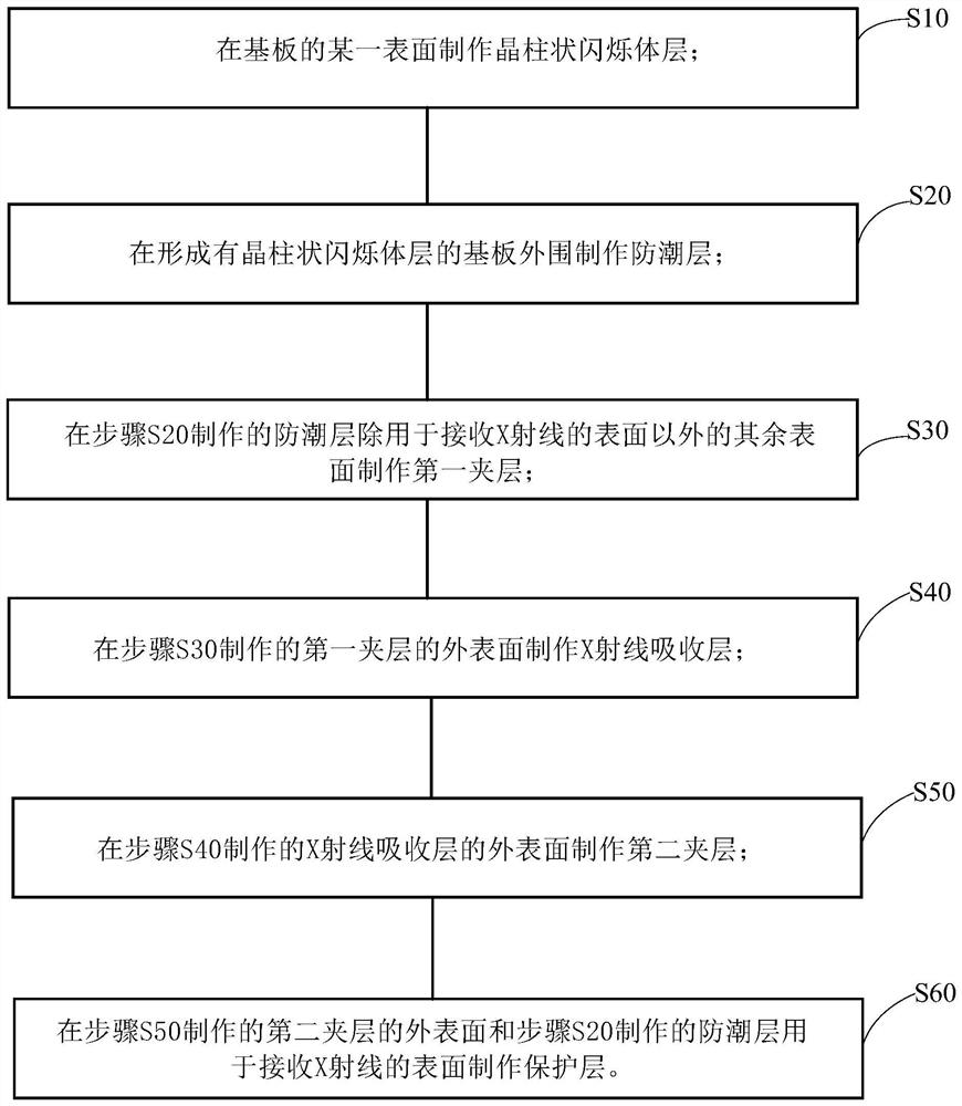
[0042] Such as figure 1 As shown, the manufacturing method of the columnar scintillation screen packaging structure includes the following steps:

[0043] Step S1: making a columnar scintillator layer on a certain surface of the substrate;

[0...


PUM


Abstract

The invention discloses a scintillation screen packaging structure, a manufacture method thereof and an image detector. The manufacture method comprises that a crystal column shaped scintillator layeris manufactured in certain surface of a substrate; a damp-proof layer is prepared in the periphery of the substrate where the crystal column shaped scintillator layer is formed; the damp-proof layeris provided with X ray absorbing layers in surface except a surface for receiving the X rays; and protective layers are made in the external surfaces of the X ray absorption layers and the surface forreceiving the X rays of the damp-proof layer. The crystal column shaped scintillator layer, damp-proof layer, X ray absorption layers and the protective layers are made successively to improve the Xray absorption rate, converted visible light transmittance and moisture resistance of the formed scintillation screen packaging structure. The X ray absorption layers are additionally arranged to absorb X rays that are not absorbed by the crystal column shaped scintillator layer, X rays of an electronic circuit of an X ray image sensor are shielded, and thus, radiation interference of the X rays in the X ray image sensor is reduced.

Description

technical field [0001] The invention relates to a manufacturing method of a cylindrical scintillation screen packaging structure (hereinafter referred to as a scintillation screen packaging structure), and also relates to a scintillation screen packaging structure and an image detector produced by the manufacturing method, belonging to the field of X-ray radiation imaging. Background technique [0002] In the industrial and medical industries, X-ray detectors are widely used, and the scintillation screen part that is indispensable for X-ray detectors is becoming more and more important. Currently commonly used scintillation screens are divided into crystal columnar scintillation screens and ceramic scintillation screens; among them, the commonly used crystal columnar scintillation screens are represented by cesium iodide, sodium iodide and other scintillation materials; this kind of scintillation screen has high brightness, high resolution, etc. Compared with ceramic scintil...

Claims


Application Information

Patent Timeline
Patent Type & Authority Patents(China)
IPC IPC(8): G01T1/202
Inventor 杨凯
Owner NANOVISION TECHNOLOGY (BEIJING) CO LTD
Why Eureka
Try Eureka