Composite current density test method and test screen of silicon wafer surface metallization interface

A test method and composite current technology, which are applied in the monitoring of photovoltaic systems, photovoltaic power generation, electrical components, etc., can solve the problems of complex cleaning process, evaluation, and difficult paste composite performance of cells, and achieve a simple test process and reduce costs. The effect of small material loss, easy slurry performance evaluation and process optimization

Inactive Publication Date: 2019-05-03
CSI CELLS CO LTD +1
View PDF7 Cites 3 Cited by
  • Summary
  • Abstract
  • Description
  • Claims
  • Application Information

AI Technical Summary

Problems solved by technology

The cleaning process of the battery sheet is complicated, and the chemical solution is consumed more; and the test result of the predetermined area of ​​the batte

Method used


Image

  • Composite current density test method and test screen of silicon wafer surface metallization interface
  • Composite current density test method and test screen of silicon wafer surface metallization interface
  • Composite current density test method and test screen of silicon wafer surface metallization interface

Examples


Embodiment Construction

[0031] The present invention will be described in detail below with reference to the embodiments shown in the accompanying drawings. However, this embodiment does not limit the present invention, and any structural, method, or functional changes made by those skilled in the art according to this embodiment are included in the protection scope of the present invention.

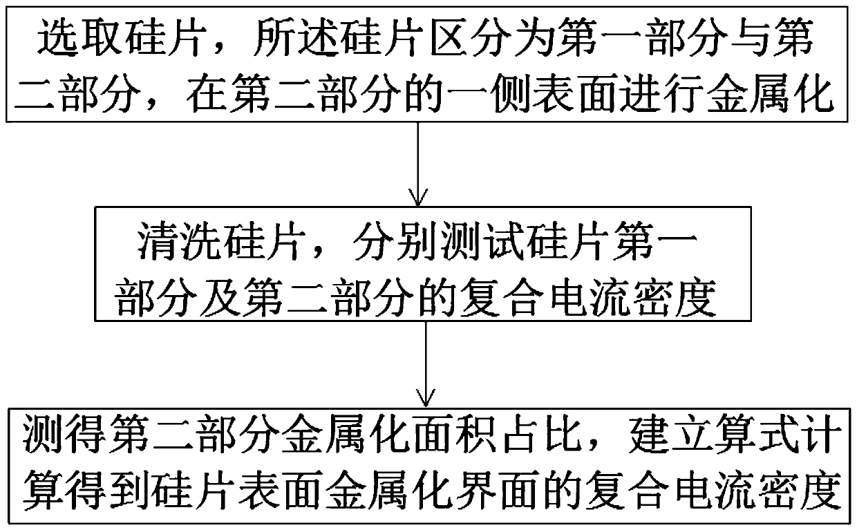
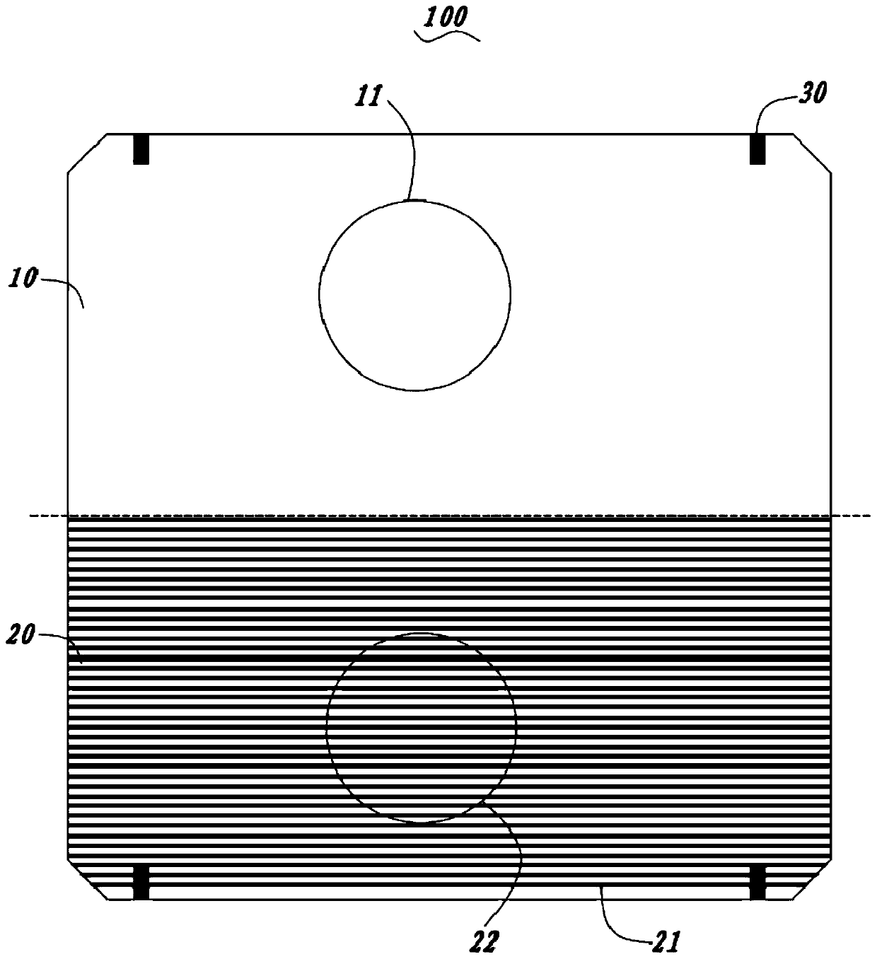
[0032] ginseng figure 1 and figure 2 As shown, the composite current density test method of the silicon chip surface metallization interface provided by the invention mainly comprises:

[0033] A silicon wafer 100 is selected, the silicon wafer 100 is divided into a first part 10 and a second part 20, and metallization is performed on one side surface of the second part 20;

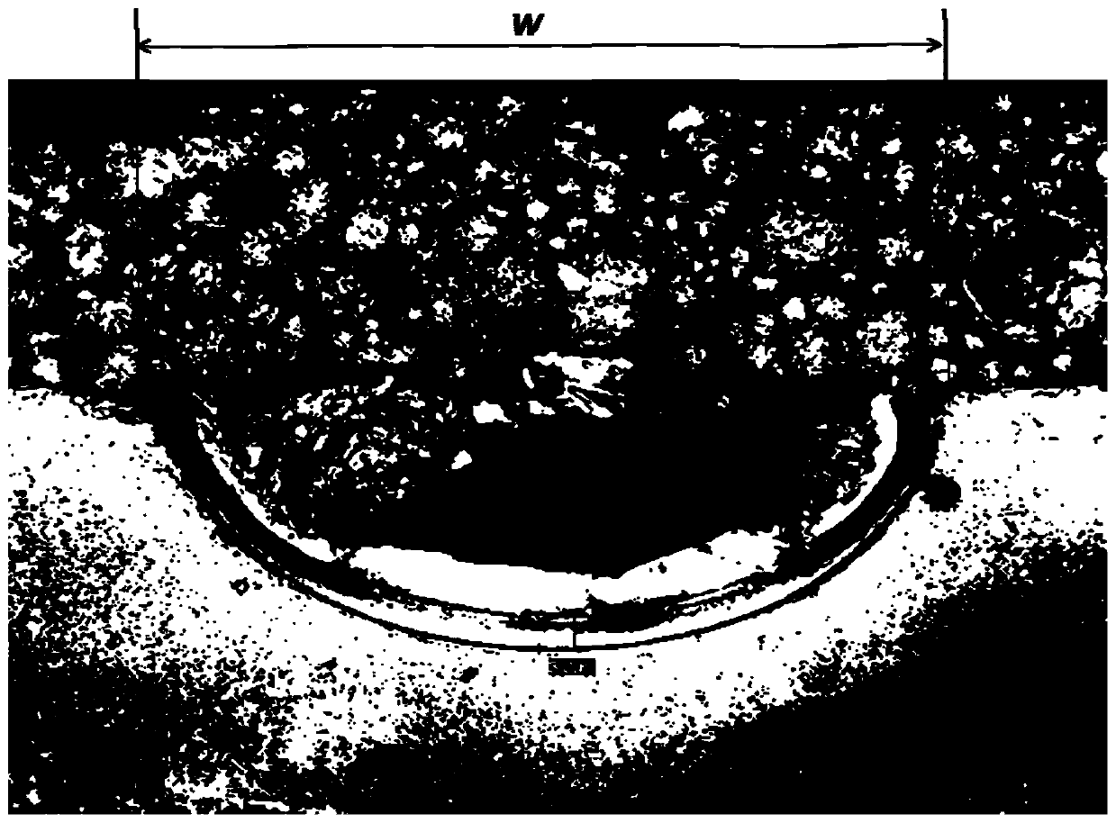
[0034] Clean the silicon wafer 100 to remove the surface metal phase and expose the metallized interface on the surface of the silicon wafer 100 to the outside, and then test separately to obtain the recombination current density J0 of ...


PUM

PropertyMeasurementUnit
Widthaaaaaaaaaa
Widthaaaaaaaaaa
Resistivityaaaaaaaaaa

Abstract

The invention provides a composite current density test method and test screen of a silicon wafer surface metallization interface, and the method comprises the steps: selecting a silicon wafer, dividing the silicon wafer into a first part and a second part, and carrying out the metallization of the surface of one side of the second part; cleaning the silicon wafer, and respectively performing testing to obtain the composite current density J0test1 of the first part and the composite current density J0test2 of the second part, wherein the composite current density J0me-Si of the silicon wafer surface metallization interface can be obtained by calculating through the J0test2 obtained through testing in combination with the composite current densities J0s1 and J0s2 of the surface of the firstpart and the metallization area proportion of the second part. According to the testing method disclosed by the invention, the composite current density J0me-Si of the silicon wafer surface metallization interface can be directly obtained by testing different positions of the silicon wafer, thereby facilitating the slurry performance evaluation and process optimization. Moreover, the test processis simpler, and the material consumption is reduced.

Description

technical field [0001] The invention relates to the technical field of photovoltaic detection, in particular to a compound current density test method and a test screen for a metallized interface on the surface of a silicon chip. Background technique [0002] With the rapid development of the photovoltaic industry, the market has put forward higher requirements for the performance and conversion efficiency of solar cells and modules. At present, crystalline silicon cells still occupy an important position in the market, and the corresponding silicon wafers are printed and sintered to obtain gate lines and realize ohmic contact. Generally, the front side of the crystalline silicon cell is screen-printed with Ag paste grid lines, and then sintered at high temperature, so that the Ag paste can burn through the SiN. x film and form a good ohmic contact with Si; the back is printed with Al paste and sintered at high temperature to form an Al-Si alloy, while part of the Al + Dop...

Claims


Application Information

Patent Timeline
IPC IPC(8): H02S50/10
CPCY02E10/50
Inventor 李硕陈瑶
Owner CSI CELLS CO LTD
Why Eureka
Try Eureka