Method for manufacturing universal backing plate of PCB solder mask plug hole

A manufacturing method and technology of plugging holes, which are applied in the fields of printed circuit manufacturing, electrical components, printed circuits, etc., can solve problems such as confusion and loss of plug hole backing plates, difficulty in finding, increasing production costs of enterprises, high manufacturing and use costs, and reduce storage costs. Cost management, production cost reduction, high versatility

Active Publication Date: 2019-05-03
KIN YIP TECHNOLDGY ELECTRONICS HUI ZHOUCO LTD
View PDF8 Cites 0 Cited by
  • Summary
  • Abstract
  • Description
  • Claims
  • Application Information

AI Technical Summary

Problems solved by technology

[0002] At present, the solder resist plugging process in the industry usually uses a special plug hole backing plate for each part number, because each part number requires special tools, including the production of drill tape data, the production of drill backing plates for drilling rigs, plate preparation, backing plate storage and use management , its production and use costs are relatively high, and there are problems such as the plug hole backing plate is easy to be confused and lost, and it is difficult to find it
According to the production cost of the drilling belt data of each backing board is 100 yuan, the labor cost of backing board production is 300 yuan, the cost of backing board material is 50 yuan, and the cost of each backing board is 450 yuan in total. If the number of backing boards is remade every day, it is counted as 3 , the monthly production cost of backing boards is 3 x 450 yuan x 30 days = 40,500 yuan, which greatly increases the production cost of the enterprise

Method used


Image

  • Method for manufacturing universal backing plate of PCB solder mask plug hole
  • Method for manufacturing universal backing plate of PCB solder mask plug hole

Examples


Embodiment 1

[0031] A method for manufacturing a PCB solder-resisting plug hole universal backing plate, comprising the following steps:

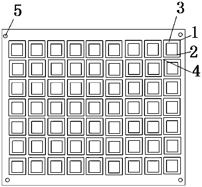
[0032] Get the substrate to be processed, the specification of the substrate is 680mm in length, 610mm in width, and 2.4mm in thickness, and the material is a fiber plate. Drill positioning holes 5 on the substrate and fix them on the gong platform with fixing pins. The positioning holes 5 are arranged on four sides of the substrate. At a corner of 5mm, the aperture is 2.05mm;

[0033] Set the specifications of the first groove according to the first stroke data, the length of the first groove 1 is 20mm, and the width is 20mm, and the first groove 1 is arranged at equal intervals along the long side and the wide side of the substrate, The distance between the adjacent first grooves 1 is 0.25mm, the depth of the first groove is adjusted to 20mm and the substrate is sunk, the depth of the sinking is 0.5mm, and the first groove 1 is obtained. The first go...

Embodiment 2

[0036] A method for manufacturing a PCB solder-resisting plug hole universal backing plate, comprising the following steps:

[0037] Get the substrate to be processed, the specification of the substrate is 700mm in length, 610mm in width, and 2.0mm in thickness, and the material is a fiber plate. Drill positioning holes 5 on the substrate and fix them on the gong platform with fixing pins. The positioning holes 5 are arranged on four sides of the substrate. At a corner of 5mm, the aperture is 2.05mm;

[0038] Set the specifications of the first groove according to the first stroke data, the length of the first groove 1 is 25mm, and the width is 25mm, and the first groove 1 is arranged at equal intervals along the long side and the wide side of the substrate, The distance between the adjacent first gong grooves is 0.25 mm, adjust the depth of the first gong knife to 18 mm and sink the substrate, the depth of the gong sinking is 0.8 mm, and the first gong groove 1 is obtained. ...

Embodiment 3

[0041] A method for manufacturing a PCB solder-resisting plug hole universal backing plate, comprising the following steps:

[0042] Get the substrate to be processed, the specification of the substrate is 720mm in length, 650mm in width, and 3.0mm in thickness, and the material is a fiber plate. Drill positioning holes 5 on the substrate and fix them on the gong platform with fixing pins. The positioning holes 5 are arranged on four sides of the substrate. At a corner of 5mm, the aperture is 2.05mm;

[0043] Set the specifications of the first groove according to the first stroke data, the length of the first groove 1 is 30mm, and the width is 20mm, and the first groove 1 is arranged at equal intervals along the long side and the wide side of the substrate, The distance between the adjacent first gong grooves 1 is 0.25 mm, adjust the depth of the first gong knife to 20 mm and sink the substrate, the sinking depth is 1.0 mm, and the first gong groove is obtained. The first go...


PUM


Abstract

The invention discloses a method for manufacturing a universal backing plate of a PCB solder mask plug hole, and the method comprises the following steps: taking a to-be-processed substrate, drillinga positioning hole in the to-be-processed substrate, and fixing the to-be-processed substrate on a gong table by using a fixing pin; setting the specification of first milling grooves according to first milling path data, wherein the first milling grooves are arranged at equal intervals along the long edge and the wide edge of the substrate; adjusting the depth of a first milling cutter, and performing the sinking milling of the substrate to obtain the first milling grooves, wherein the first milling grooves are arranged in a grid shape; and setting the specification of second milling groovesaccording to the second milling process data, wherein the specification of the second milling grooves are smaller than the specification of the first milling grooves; adjusting the depth of a second milling cutter, and milling through the substrate in the first milling grooves according to the specification of the second milling grooves. The method has the advantages that the manufacturing steps are simple, the manufactured base plate is high in universality, the manufacturing cost and the storage management cost of the hole plugging base plate are greatly reduced, and production, operation and use are facilitated.

Description

technical field [0001] The invention relates to the field of printed circuit boards, in particular to a method for manufacturing a PCB solder-resisting plug hole universal backing plate. Background technique [0002] At present, the solder resist plugging process in the industry usually uses a special plug hole backing plate for each part number, because each part number requires special tools, including the production of drill tape data, the production of drill backing plates for drilling rigs, plate preparation, backing plate storage and use management , its production and use costs are higher, and there are problems such as that the backing plate of the plug hole is easy to be confused and lost, and it is difficult to find it. According to the production cost of drill belt data for each backing board is 100 yuan, the labor cost of backing board production is 300 yuan, the cost of backing board material is 50 yuan, and the cost of each backing board is 450 yuan in total. I...

Claims


Application Information

Patent Timeline
Patent Type & Authority Applications(China)
IPC IPC(8): H05K3/00
Inventor 林伟玉
Owner KIN YIP TECHNOLDGY ELECTRONICS HUI ZHOUCO LTD
Why Eureka
Try Eureka