Driving device for active matrix organic light emitting diode display and manufacturing method thereof

a technology of organic light-emitting diodes and driving devices, which is applied in the direction of semiconductor devices, instruments, optics, etc., can solve the problems of oled device deterioration, limited size of passive matrix oled, and shorter life and deterioration of oled devices, so as to achieve less leakage current, improve emissive efficiency, and simple production procedure

Inactive Publication Date: 2006-01-19
INNOLUX CORP
View PDF9 Cites 21 Cited by
  • Summary
  • Abstract
  • Description
  • Claims
  • Application Information

AI Technical Summary

Benefits of technology

[0007] In view of the foregoing, the present invention provides a new driving device for an active matrix OLED display and its manufacturing method. The new structure of the driving device is implemented by forming the pixel electrode directly on a substrate surface by means of a simple production procedure.
[0008] The driving device comprises a substrate, a dielectric layer, a thin-film transistor, and a transparent conductive layer. The dielectric layer is formed above the substrate and covers the source and the drain of the thin-film transistor. Source and drain electrode pass through the dielectric layer for separately connecting with the source and drain area. The transparent conductive layer gets direct contact with the substrate and is connected to the drain through the drain electrode, so the transparent conductive layer can be functioned as a pixel electrode. The driving device provides the less leakage current and higher emissive efficiency than the prior active matrix displays.
[0009] The present invention also provides a method of manufacturing the driving device for the active matrix OLED display which can simplify process. The method of manufacturing the driving device includes the steps of: providing a substrate; forming a thin-film transistor above the substrate; providing a dielectric layer to cover the source and the drain of the thin-film transistor; forming a contact area that exposes the substrate and holes connecting the source and the drain by executing a photolithography process; filling holes with a conductive layer and form the source electrode and the drain electrode; and forming a transparent conductive layer that directly contact with the substrate through the contact area and is connected to the drain through the drain electrode. Because of the characteristics of the structure, the present invention provides easier manufacturing steps than the prior art of active matrix displays. The present invention uses photolithography process to form separately the contact area, the source and the drain connection holes in the driving device by several steps or one step. Thus, it decreases the amount of masks and the steps of the photolithography process. The present invention can be complete by the current production equipments and there is no need to acquire new equipment.

Problems solved by technology

The disadvantage of the passive matrix OLED is the size limitation.
To develop the large size passive matrix displays has some problems such as higher energy consumption, shorter lifetime and deterioration of the OLED device.
Active matrix displays formed by the structure described above have low emissive efficiency and larger leakage current than passive matrix displays.

Method used


Image

  • Driving device for active matrix organic light emitting diode display and manufacturing method thereof
  • Driving device for active matrix organic light emitting diode display and manufacturing method thereof
  • Driving device for active matrix organic light emitting diode display and manufacturing method thereof

Examples


first embodiment

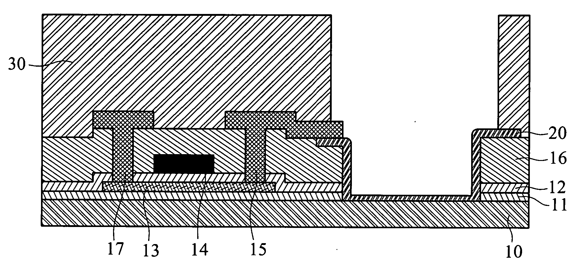
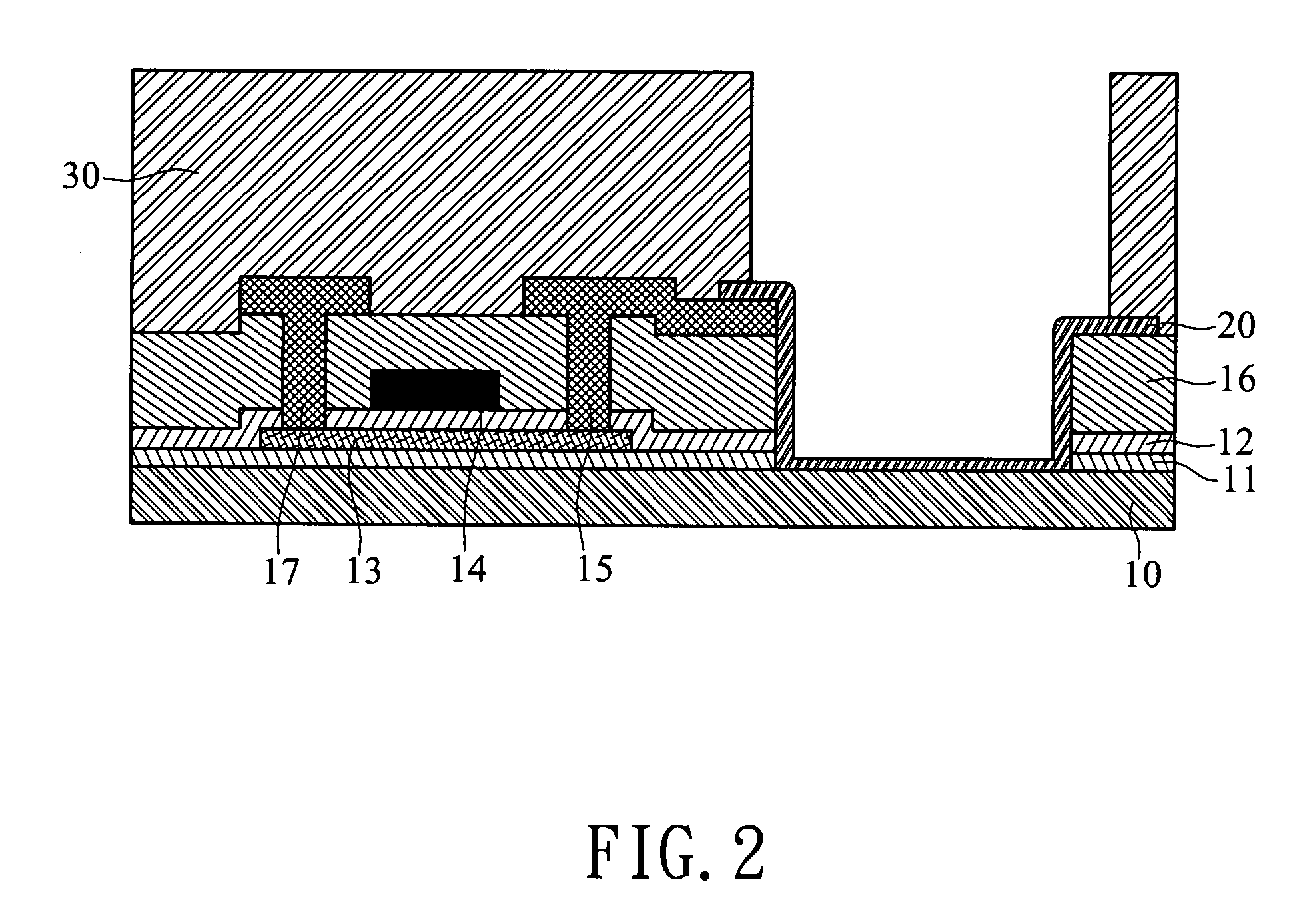
[0016] Referring to FIG. 2, a schematic view of a first embodiment according to the present invention is illustrated. An insulated substrate is made up of a substrate 10 and a buffering layer 11. A poly-Si layer 13 is deposited on the surface of the buffering layer 11. A drain, a source, and a channel of a thin-film transistor are defined in the poly-Si layer 13. An insulating layer 12 covers the buffering layer 11 and the poly-Si layer 13. A gate 14 is isolated by the insulating layer 12 and located on the top of the channel in the thin-film transistor. A dielectric layer 16 covers the surface of the gate 14. The dielectric layer 16 and the insulating layer 12 are each provided with connection holes going through to the source and the drain. The connection holes are filled with conductive materials and form the source electrode 17 and the drain electrode 15. A transparent conductive layer 20 contacts the substrate 10 directly, and is connected to the drain through the drain electro...

second embodiment

[0019] The transparent conductive layer can be provided either above or below the extended part of the drain electrode, referring to FIG. 4, a schematic view of a second embodiment according to the present invention is illustrated. The transparent conductive layer is provided below an extended part of the drain electrode.


PUM

PropertyMeasurementUnit
transparentaaaaaaaaaa
dielectricaaaaaaaaaa
voltageaaaaaaaaaa

Abstract

A driving device for an active matrix OLED display is disclosed, wherein a pixel electrode is directly contact the substrate, and the pixel electrode is connected electrically to the drain of the thin-film transistor through a drain electrode. Such a device decreases a leakage current and increases emission efficiency. A method of manufacturing the driving device is also disclosed.

Description

BACKGROUND OF THE PRESENT INVENTION [0001] 1. Field of Invention [0002] The invention relates to an active matrix organic light emitting diode display and the manufacturing method of the same. In particular, it relates to a driving device for an organic light emitting diode display and manufacturing method of the same. [0003] 2. Related Art [0004] As the technology of thin-film transistor liquid crystal display (TFT LCD) improves, flat screen displays become the mainstream products on the display market. The development of liquid crystal display industry increases the quality and yield of the displays, and also accelerates expectations and demands for the next generation displays. The organic light emitting diode (OLED) display has the features of light, thin, low driving voltage, self-emissive and wide viewing angles. The manufacturing process for the OLED display is also simpler than the LCD displays and the OLED easily applies to flexible displays. It is the next generation displ...

Claims


Application Information

Patent Timeline
Patent Type & Authority Applications(United States)
IPC IPC(8): G02F1/1343
CPCH01L27/3248H10K59/123
Inventor TSAI, YAW-MINGCHANG, SHIH-CHANG
Owner INNOLUX CORP
Why Eureka
Try Eureka