Gold nano structure with cone-shaped surface and preparation method and application thereof
A gold nanostructure and gold nanoparticle technology is applied in nanotechnology, nanotechnology, nanotechnology, etc. for materials and surface science. Weak force and other problems, to achieve the effect of stable structure, scientific preparation method, high SERS activity
- Summary
- Abstract
- Description
- Claims
- Application Information
AI Technical Summary
Benefits of technology
Problems solved by technology
Method used
Image
Examples
Embodiment 1
[0043] The concrete steps of preparation are:
[0044] Step 1, first according to the weight ratio of chloroauric acid powder, polyvinylpyrrolidone powder, citric acid powder and water is 0.04:1.2:0.0005:55, the chloroauric acid powder, polyvinylpyrrolidone powder and citric acid powder are dissolved in water to obtain a mixture. Then the mixed solution was heated to 35° C. and kept for 6 hours to obtain an electrolyte solution.
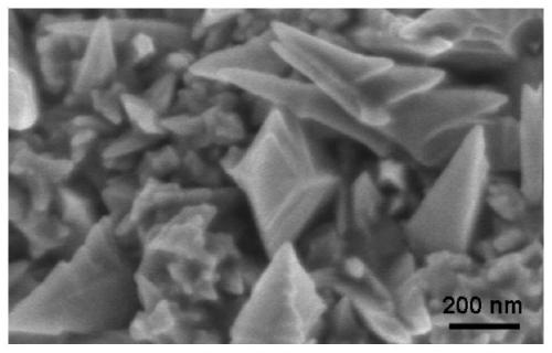
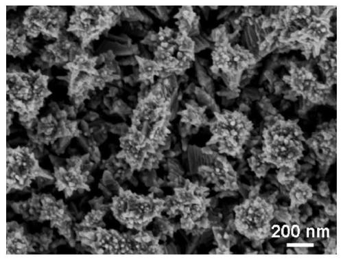
[0045] In step 2, an 18nm-thick gold film is sputtered on the conductive substrate; wherein, the conductive substrate is a single crystal silicon wafer conductive substrate. Then, the conductive substrate covered with gold film was used as the cathode, and the graphite sheet was used as the anode, and they were placed together in the electrolyte solution at 35°C, and the current density was 60μA / cm 2 Electrodeposited at a constant current for 9h to obtain a conductive substrate covered with pointed cone-shaped particles.
[0046]In step 3, the ele...
Embodiment 2
[0048] The concrete steps of preparation are:
[0049] Step 1, first according to the weight ratio of chloroauric acid powder, polyvinylpyrrolidone powder, citric acid powder and water is 0.045:1.1:0.00075:53, the chloroauric acid powder, polyvinylpyrrolidone powder and citric acid powder are dissolved in water to obtain a mixture. Then, the mixed solution was heated to 39° C. and kept for 5.2 hours to obtain an electrolyte solution.
[0050] In step 2, a gold film with a thickness of 19 nm is sputtered on the conductive substrate; wherein, the conductive substrate is a single crystal silicon wafer conductive substrate. Then, the conductive substrate covered with gold film was used as the cathode, and the graphite sheet was used as the anode, and they were placed together in the electrolyte solution at 39°C, and the current density was 75μA / cm 2 Electrodeposited at a constant current for 8h to obtain a conductive substrate covered with pointed cone-shaped particles.
[0051...
Embodiment 3
[0053] The concrete steps of preparation are:
[0054] Step 1, according to the weight ratio of chloroauric acid powder, polyvinylpyrrolidone powder, citric acid powder and water is 0.05:1:0.001:50, dissolve the chloroauric acid powder, polyvinylpyrrolidone powder and citric acid powder in water to obtain a mixture. Then the mixed solution was heated to 43° C. and kept for 4.5 hours to obtain an electrolyte solution.
[0055] Step 2, sputtering a 20nm-thick gold film on the conductive substrate; wherein, the conductive substrate is a single crystal silicon wafer conductive substrate. Then, the conductive substrate covered with gold film was used as the cathode, and the graphite sheet was used as the anode, and they were placed together in the electrolyte solution at 43°C, and the current density was 90μA / cm 2 Electrodeposited at a constant current for 7h to obtain a conductive substrate covered with pointed cone-shaped particles.
[0056] In step 3, the electrolyte solution...
PUM
 Abstract
Description
Claims
Application Information


