On-chip detection system and test method for identifying aged and recycled integrated circuit

An on-chip detection and integrated circuit technology, which is applied in the direction of electronic circuit testing, etc., can solve the problems of high use and testing costs for users, inability to detect chip performance status, and insufficient detection or identification accuracy.

Inactive Publication Date: 2019-05-07
BEIHANG UNIV
View PDF1 Cites 6 Cited by
  • Summary
  • Abstract
  • Description
  • Claims
  • Application Information

AI Technical Summary

Problems solved by technology

[0004] ① The area and power consumption are too large;
[0005] ② The detection or recognition accuracy is not high enoug

Method used


Image

  • On-chip detection system and test method for identifying aged and recycled integrated circuit
  • On-chip detection system and test method for identifying aged and recycled integrated circuit
  • On-chip detection system and test method for identifying aged and recycled integrated circuit

Examples


Embodiment Construction

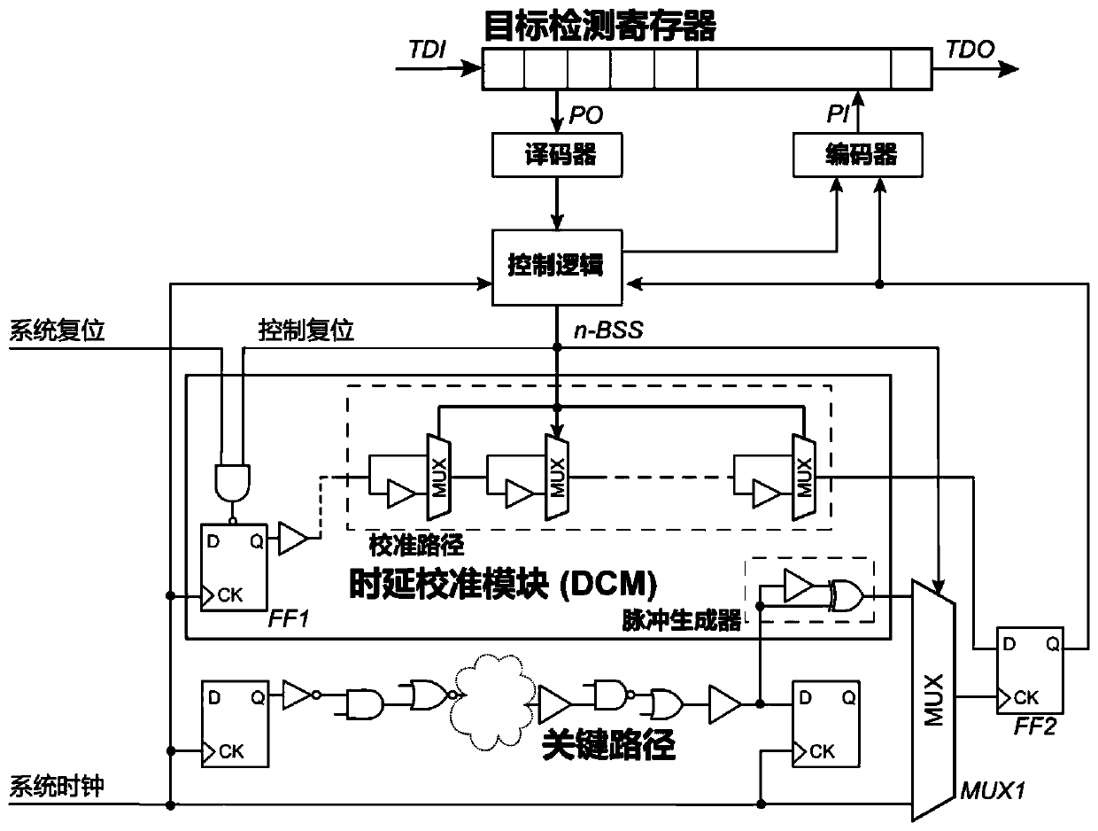
[0029] The following will introduce the specific operation flow and implementation of the burn-in recycling integrated circuit on-chip detection system designed in the present invention with reference to the accompanying drawings.

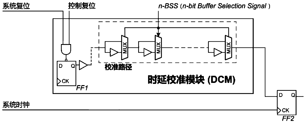
[0030] Step 1: The tester and the user configure the target detection register (hereinafter referred to as TDR) through the JTAG test access port (hereinafter referred to as TAP), and determine the logical value stored in each register in the TDR. The instructions and test data vectors (hereinafter referred to as TDV) inside the TDR are decoded by the control logic of the peripheral control circuit and output the n-level buffer selection signal (hereinafter referred to as n-BSS) to control the number of buffers (Buffer) connected to the calibration path. . Wherein the n-BSS signal will be used in the off-chip detection process of the subsequent step 4.

[0031] Step 2: The delay calibration module not only needs to be calibrated by the clock signa...


PUM


Abstract

The invention discloses an on-chip detection system and a test method for identifying aged and recycled integrated circuit. The system comprises a test data register, a peripheral circuit, a delay calibration module, a clock path, and a critical path. The method comprises: step 1, configuring the test data register; step 2, calibrating a calibration path in the delay calibration module; step 3, outputting a calibration result as a test data vector; step 4, solving an aging time according to a theoretical model; and step 5, performing an off-chip test flow. The advantages of the present invention are that: the area and the power consumption cost are small; the system can be easily deployed on a large-scale integrated circuit and used as an on-chip test structure; the error for identifying the aging time that the aged and recycled integrated circuit experienced is small and no more than 30 days; the test precision of the delay calibration module is very high and can reach 15 ps; and theworking performance of the chip in the current aging state can be detected.

Description

technical field [0001] The invention relates to an on-chip detection system and test method for identifying aging and recycled integrated circuits, especially an on-chip detection system and test method that can identify aging or recycled integrated circuits by means of path delay calibration. Design For Test (Design For Test) field. Background technique [0002] In recent years, more and more counterfeit integrated circuits (Counterfeit Integrated Circuit) have flowed into the supply chain of electronic components. This not only brings economic losses to integrated circuit design and manufacturers, but also brings major security threats and hidden dangers to users. Counterfeiting integrated circuits has become a common concern of the government and the entire electronic information industry. More than 80% of the counterfeit integrated circuits are aging recycled integrated circuits, and aging recycled integrated circuits are bound to be affected by aging effects such as n...

Claims


Application Information

Patent Timeline
IPC IPC(8): G01R31/28
Inventor 王晓晓汝松昊
Owner BEIHANG UNIV
Why Eureka
Try Eureka