A DRAM output driving circuit and a method for reducing electric leakage thereof

A technology for outputting driving circuits and voltages, applied in the field of DRAM output driving circuits, can solve the problem of large leakage of output stage driving circuits, and achieve the effects of reducing leakage current, reducing leakage current, and reducing leakage current.

Inactive Publication Date: 2019-05-10
XI AN UNIIC SEMICON CO LTD
View PDF9 Cites 1 Cited by
  • Summary
  • Abstract
  • Description
  • Claims
  • Application Information

AI Technical Summary

Problems solved by technology

However, in the low power circuit design, the leakage of the device in the off state needs to be considered. Therefore, in the power saving mode of the DRAM memory in the prior art, the leakage of the output stage driving circuit is too large to meet the actual requirements. Require

Method used


Image

  • A DRAM output driving circuit and a method for reducing electric leakage thereof
  • A DRAM output driving circuit and a method for reducing electric leakage thereof
  • A DRAM output driving circuit and a method for reducing electric leakage thereof

Examples


Embodiment 1

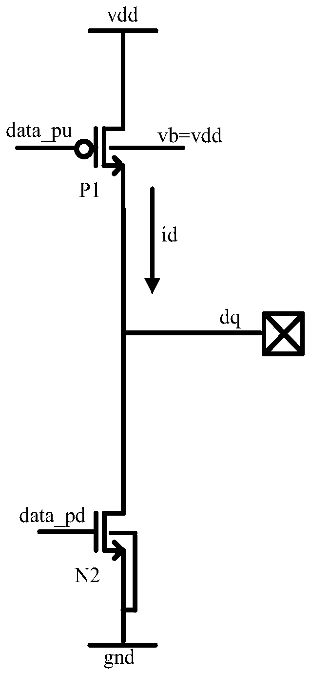
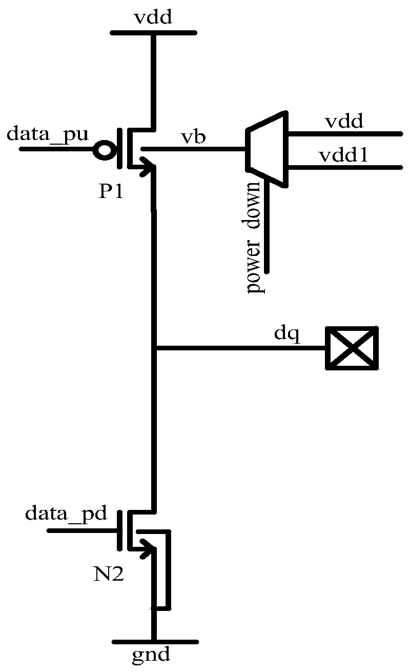
[0023] In this embodiment, when the pull-up transistor of the DRAM output driving circuit is a PMOS.

[0024] The base voltage vb is not directly connected to the working voltage vdd, but is connected to the output of the voltage selector. The input of the voltage selector is the working voltage vdd and the extra working voltage vdd1. Power_down is a voltage selection signal. The extra working voltage vdd1 is a voltage higher than the working voltage vdd.

[0025] Normal working mode: power_down=0, vb=vdd.

[0026] Power saving mode: power_down=1, data_pu=vdd, data_pd=gnd, dq=gnd, vb=vdd1, where vdd1 is a higher voltage than vdd.

[0027] In the power-saving mode, the threshold voltage of the PMOS transistor P1 becomes lower due to the rise of vb, because the leakage current of the PMOS transistor is positively correlated with the threshold voltage, so the leakage current from vdd to dq through P1 becomes smaller. In the normal working mode, vb=vdd, the threshold voltage o...

Embodiment 2

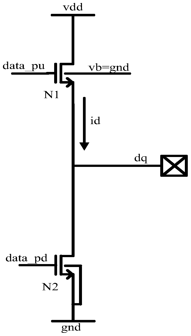
[0029] In this embodiment, the pull-up transistor of the DRAM output driving circuit is NMOS.

[0030] The base voltage vb is not directly connected to the ground voltage gnd, but is connected to the output of the voltage selector. The input of the voltage selector is the ground voltage gnd and the extra ground voltage v_neg. Power_down is a voltage selection signal. Wherein the additional ground voltage v_neg is a voltage lower than the ground voltage gnd.

[0031] Normal working mode: power_down=0, vb=gnd.

[0032] Power saving mode: power_down=1, data_pu=gnd, data_pd=gnd, dq=gnd, vb=v_neg, v_neg is a lower voltage than gnd.

[0033] In the power-saving mode, the threshold voltage of the NMOS transistor N1 increases due to the drop of vb, because the leakage current of the NMOS transistor is negatively correlated with the threshold voltage, so the leakage current from vdd to dq through N1 becomes smaller . In the normal working mode, vb=gnd, the threshold voltage of the...


PUM


Abstract

The DRAM output driving circuit comprises a pull-up transistor and a pull-down transistor which are sequentially connected to a working voltage end and a grounding voltage end, and a driving voltage output end dq is arranged between the pull-up transistor and the pull-down transistor; wherein the substrate of the pull-up transistor is connected with the output end of the voltage selector, the input end of the voltage selector is respectively connected with corresponding loading voltage and additional loading voltage, and the control end of the voltage selector is connected with a voltage selection signal. The voltage selector is arranged to aim at different pull-up transistors; Substrate voltages of different sizes are selected under different states, so that the leakage current of the output driving circuit can be reduced in a power-saving mode according to the correlation between the leakage current of different pull-up transistors and threshold voltage, the electric leakage is reduced, and enough driving capability can be provided for an output stage under the condition of normal work; and the leakage current of the DRAM output driving circuit in a power-saving mode is effectively reduced.

Description

technical field [0001] The invention relates to a DRAM output driving circuit, in particular to a DRAM output driving circuit and a method for reducing electric leakage. Background technique [0002] In the prior art, the output driver circuit of the DRAM memory includes the following two types according to the type of the pull-up transistor: one is when the pull-up transistor is PMOS, that is, P1, such as figure 1 shown. In the power saving mode of DRAM, the dq pin is connected to gnd, and the connection state of PMOS is: vb=vdd; power saving mode: dat_pu=vdd, data_pd=gnd, dq=gnd; although P1 does not have when vsg=0v It is turned on, and there is still leakage from vdd to dq, which is determined by the device characteristics, where vsg refers to the source and gate voltage difference of P1. The other is when the pull-up transistor is NMOS, namely N1, such as figure 2 shown. In the power saving mode of DRAM, the dq pin is connected to gnd, and the connection state of N...

Claims


Application Information

Patent Timeline
Patent Type & Authority Applications(China)
IPC IPC(8): G11C11/4096
Inventor 刘成白亮向荣
Owner XI AN UNIIC SEMICON CO LTD
Why Eureka
Try Eureka