A storage chip SUBROM detection method and a detector
A memory chip and detection method technology, applied in static memory, instruments, etc., can solve the problems of low detection efficiency and achieve the effect of improving detection efficiency and fast and accurate detection of qualification
- Summary
- Abstract
- Description
- Claims
- Application Information
AI Technical Summary
Problems solved by technology
Method used
Image

Examples
Embodiment 1
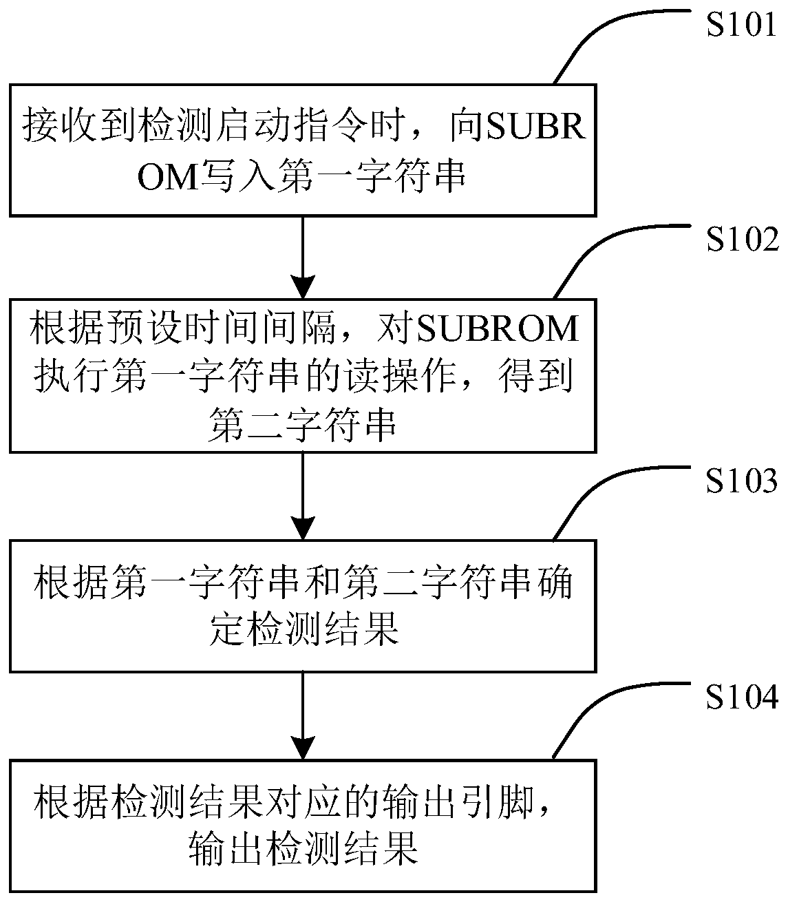
[0047] The embodiment of the present invention provides a storage chip SUBROM detection method, such as figure 1 As shown, the method includes the following steps:
[0048] S101: When a detection start instruction is received, write a first character string into the SUBROM.
[0049] Wherein, the detection start instruction is an instruction for starting detection. When receiving the instruction to start the detection, write the first character string into the storage chip SUBROM to be detected. In an implementation manner, the detection start instruction may be triggered by a user (also known as a detection person) according to a detection requirement. For example, after the user connects the SUBROM to the SUBROM detector, the user clicks or presses a test control switch provided by the SUBROM detector to trigger a detection start instruction. Users can control the startup time of SUBROM according to their own schedule. For example, when the user is tired, he can close his...
Embodiment 2
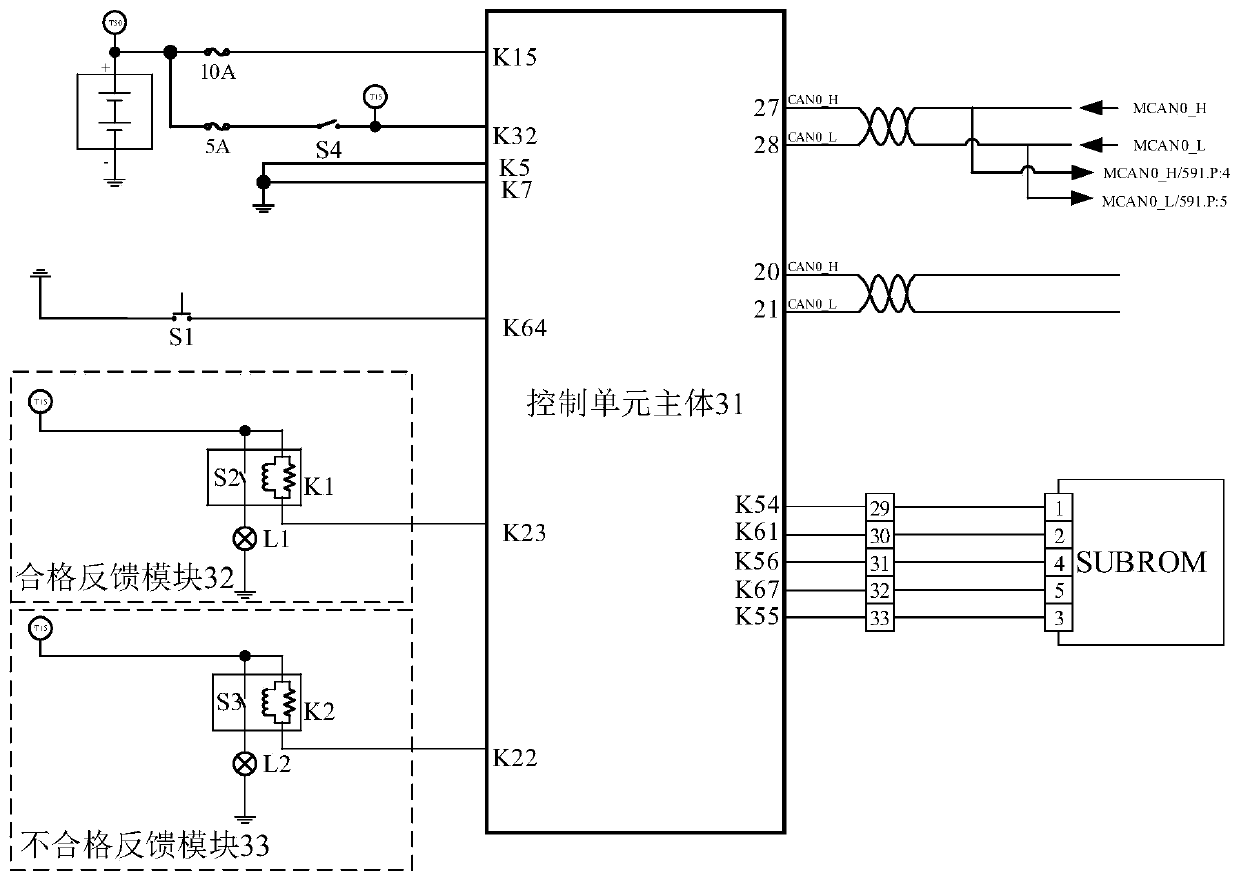
[0083] An embodiment of the present invention provides a memory chip SUBROM detector, such as figure 2 As shown, it includes: control unit main body 31, qualified feedback module 32, unqualified feedback module 33, test control switch S1; the control unit main body includes test input pins, first output pins, second output pins, read and write data pin. The test input pin can be the K64 pin of the control unit main body 31, the first output pin can be the K23 pin of the control unit main body, the second output pin can be the K22 pin of the control unit main body 31, and the read and write data reference The pin can be the K67 pin of the main body 31 of the control unit. The control unit body 31 may be an automatic transmission control unit (Transmission Control Unit, TCU).
[0084] The pin K64 of the control unit main body 31 is connected to the test control switch S1, and the test control switch S1 is used for inputting a detection start instruction. The test control swi...
Embodiment 3
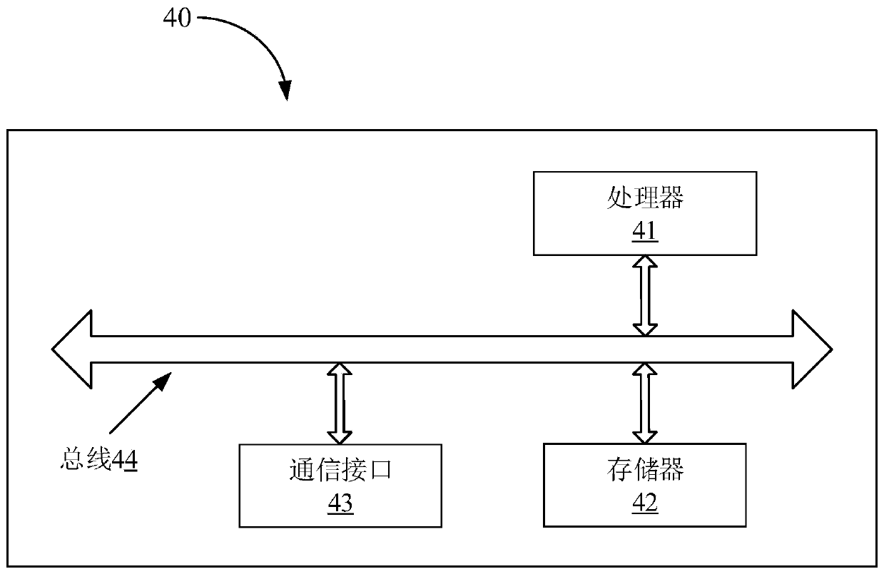
[0095] An electronic device provided by an embodiment of the present invention, such as image 3 As shown, the electronic device 40 includes a processor 41 and a memory 42, the memory stores a computer program that can run on the processor, and the processor implements the method provided by the first embodiment above when executing the computer program A step of.
[0096] see image 3 , the electronic device further includes: a bus 44 and a communication interface 43 , the processor 41 , the communication interface 43 and the memory 42 are connected through the bus 44 . The processor 41 is used to execute executable modules, such as computer programs, stored in the memory 42 .
[0097] Wherein, the memory 42 may include a high-speed random access memory (RAM, Random Access Memory), and may also include a non-volatile memory (non-volatile memory), such as at least one disk memory. The communication connection between the system network element and at least one other network...
PUM
 Abstract
Description
Claims
Application Information