Memory and method of forming the same

A memory, wet etching technology, applied in semiconductor devices, electrical solid devices, electrical components, etc., can solve problems affecting memory performance, changes in electrical parameters such as resistance, achieve uniform thickness, improve yield, and improve performance Effect

Active Publication Date: 2021-05-18
YANGTZE MEMORY TECH CO LTD
View PDF2 Cites 0 Cited by
  • Summary
  • Abstract
  • Description
  • Claims
  • Application Information

AI Technical Summary

Problems solved by technology

[0004] In the prior art, the sacrificial layer is usually removed by a wet etching process, but in the prior art, after the sacrificial layer is removed, it is often found that the thickness of the insulating layer gradually increases from top to bottom, eventually making the The thickness of the control gate layer formed between adjacent insulating layers gradually decreases from top to bottom, so that the electrical parameters such as resistance between the control gates of each memory cell change, which in turn affects the performance of the entire memory

Method used


Image

  • Memory and method of forming the same
  • Memory and method of forming the same
  • Memory and method of forming the same

Examples


Embodiment Construction

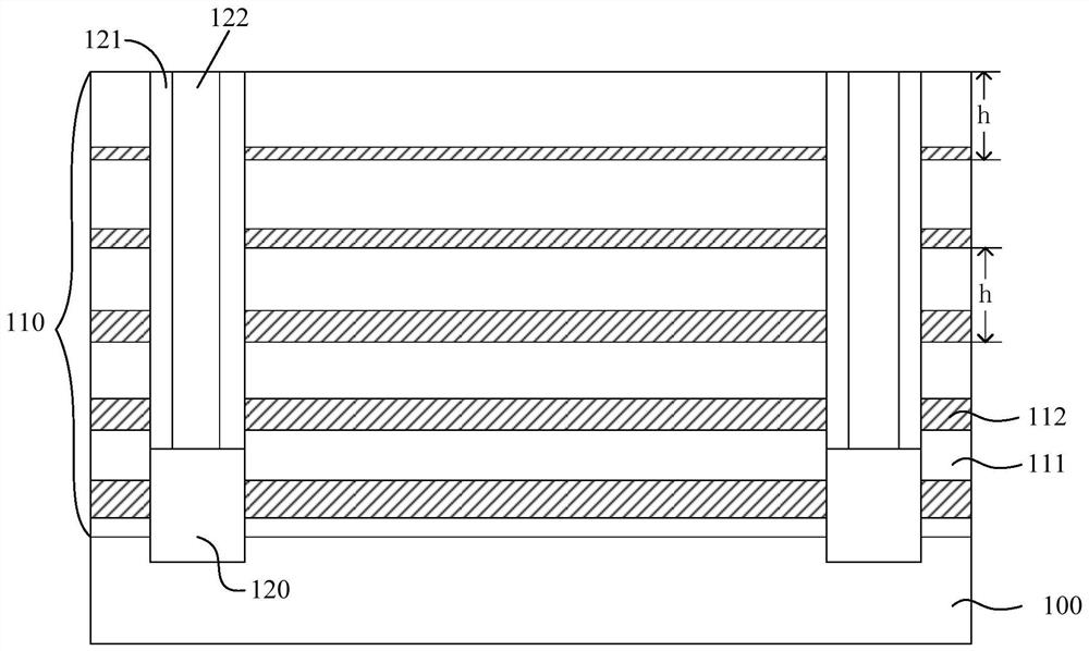
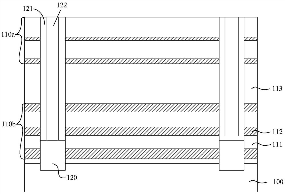
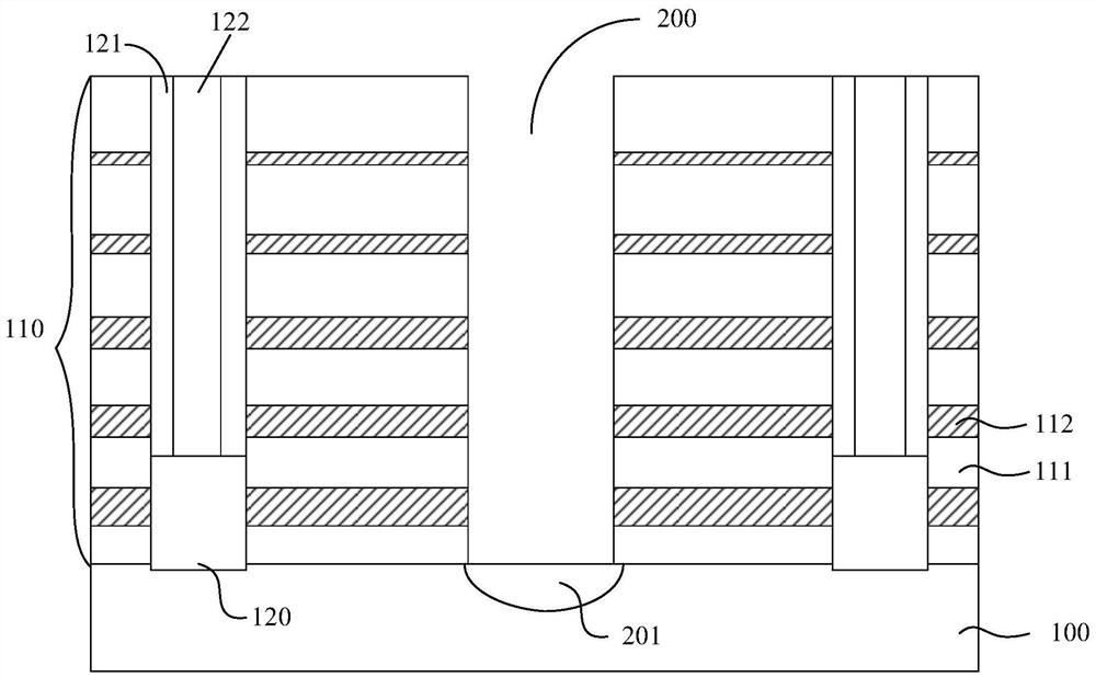
[0026] As mentioned in the background art, after removing the sacrificial layer in the prior art, the problem of non-uniform thickness of the insulating layer tends to occur.

[0027] The study found that, due to the large thickness of the stacked structure on the substrate surface, the depth of the gate line spacer groove formed before removing the sacrificial layer is relatively large. Although the etching solution has a high etching selectivity for the sacrificial layer during the wet etching process, it also causes etching to a certain extent for the insulating layer. During the wet etching process, the exchange rate of the etching solution near the top of the grid line spacer is greater than the exchange rate of the etching solution near the bottom of the grid line spacer, resulting in the grid line The concentration of silicon in the etching solution in the spacer gradually increases from the top of the stack structure downward, so that the etching rate of the insulating...


PUM


Abstract

The present invention relates to a memory and its forming method. The forming method of the memory includes: providing a substrate, forming a stack structure on the surface of the substrate, the stack structure including alternately stacked insulating layers and sacrificial layers, the insulating The thickness of the layer gradually increases from the surface of the substrate; etching the stacked structure to the surface of the substrate to form a gate line spacer that runs through the stacked structure; using a wet etching process, along the gate line spacer, removing the sacrificial layer, during the process of removing the sacrificial layer, the etching amount of the insulating layer by the wet etching process gradually increases from the surface of the substrate, and the change of the thickness of the insulating layer is used for The variation of the etching amount of the insulating layer is offset. The thickness of the insulating layer of the storage memory formed by the method is uniform, which is beneficial to improving the product yield.

Description

technical field [0001] The invention relates to the technical field of semiconductors, in particular to a memory and a forming method thereof. Background technique [0002] In recent years, the development of flash memory (Flash Memory) is particularly rapid. The main feature of flash memory is that it can keep stored information for a long time without power on, and has the advantages of high integration, fast access speed, easy erasing and rewriting, etc. Has been widely used. In order to further increase the bit density (Bit Density) of the flash memory while reducing the bit cost (Bit Cost), three-dimensional flash memory (3D NAND) technology has been developed rapidly. [0003] In the process of forming a 3D NAND memory, it is necessary to form a stacked structure of a sacrificial layer and an insulating layer on the surface of the substrate, and then form a gate line spacer through the stacked structure, and then remove the sacrificial layer along the gate line space...

Claims


Application Information

Patent Timeline
Patent Type & Authority Patents(China)
IPC IPC(8): H01L27/1157H01L27/11578H01L21/28H01L29/423
Inventor 苏界徐融孙文斌
Owner YANGTZE MEMORY TECH CO LTD
Why Eureka
Try Eureka